Video: Advanced Packaging for Next-Generation Semiconductors
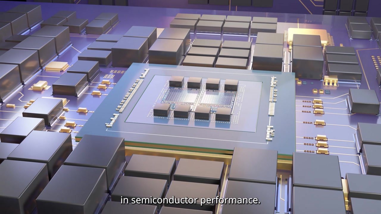
Feb 02, 2026Advanced packaging enables faster, more efficient devices by integrating compute and memory chips for artificial intelligence (AI), data centers, autonomous vehicles and mobile devices. New architectures increase manufacturing complexity. With more designs per package, yield management becomes critical. The performance of each package relies on the integrity of every chip. With billions of chips powering trillions of interactions daily, manufacturers have zero margin for error. Through KLA’s portfolio of process and process control solutions for wafers, panels and components, we help our customers optimize every step of the packaging process, shaping the future of semiconductor innovation in the AI age.


