3D Optical Profilometers

3D Optical Profilometers
The Profilm3D® benchtop optical profiler and Zeta™ optical profilometers are non-contact surface profilers that provide fast, easy, 3D surface topography measurements. As a leading non-contact profilometer solution, our portfolio of 3D optical profilers supports a variety of measurement techniques, including white light interferometry, True Color imaging and ZDot™ confocal grid structured illumination. KLA Instruments can help guide you to the right 3D optical profiler solution for your unique measurement needs.
Products
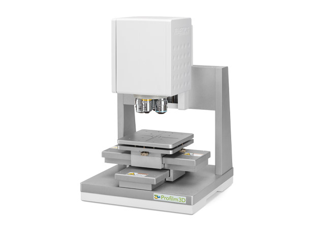
Filmetrics® Profilm3D® Optical Profilometer
The Profilm3D® benchtop optical profiler utilizes white light interferometry, TotalFocus® infinite depth-of-field imaging, or Enhanced Roughness Mode to provide easy, non-contact measurement of 3D step heights, roughness, and other surface topography.

Zeta™-Solar Metallization Optical Profiler
The new Zeta-Solar non-contact optical profiler is a metrology tool designed for measuring 3D topography for advanced metallization finger, busbar and pad solar processes. A large sample stage and automated analysis recipes with pass/fail criteria make the Zeta-Solar ideal for end-of-the-line solar process development and process quality control.
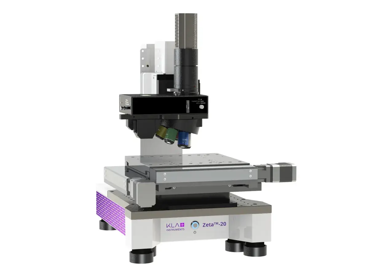
Zeta™-20 Optical Profiler
The Zeta-20 benchtop 3D non-contact optical profilometer features patented ZDot™ technology and flexible multi-mode optics for measurement of 3D surface topography, film thickness and automated defect inspection. The High Resolution HR configuration is designed specifically for advanced solar applications.
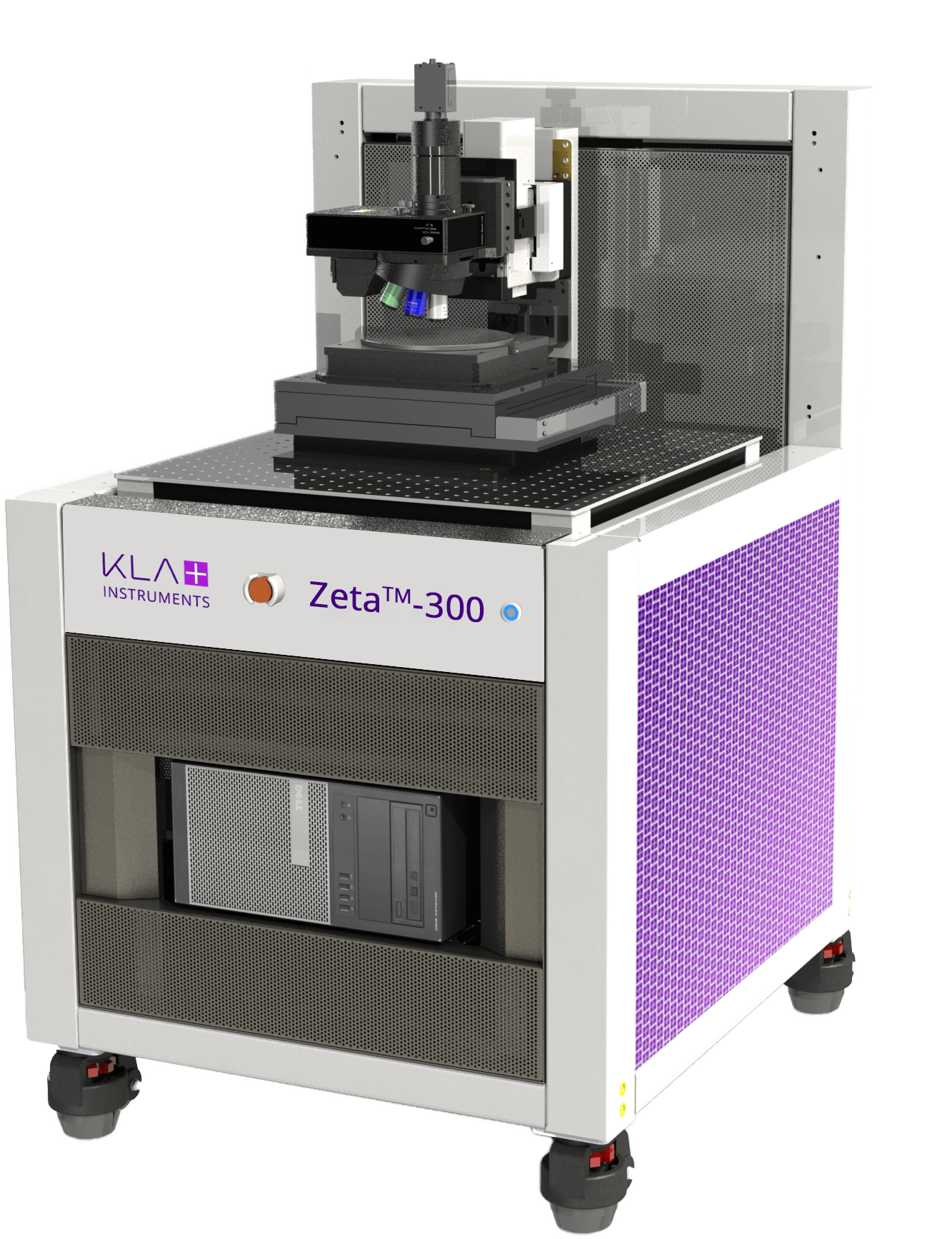
Zeta™-300 Optical Profiler
Building upon the proven performance of the Zeta-20, the Zeta-300 non-contact 3D optical profiler includes integrated vibration isolation and support for larger sample sizes to meet your R&D and production requirements. The non-contact profilometer integrates six different optical metrology technologies in one configurable and easy-to-use system.
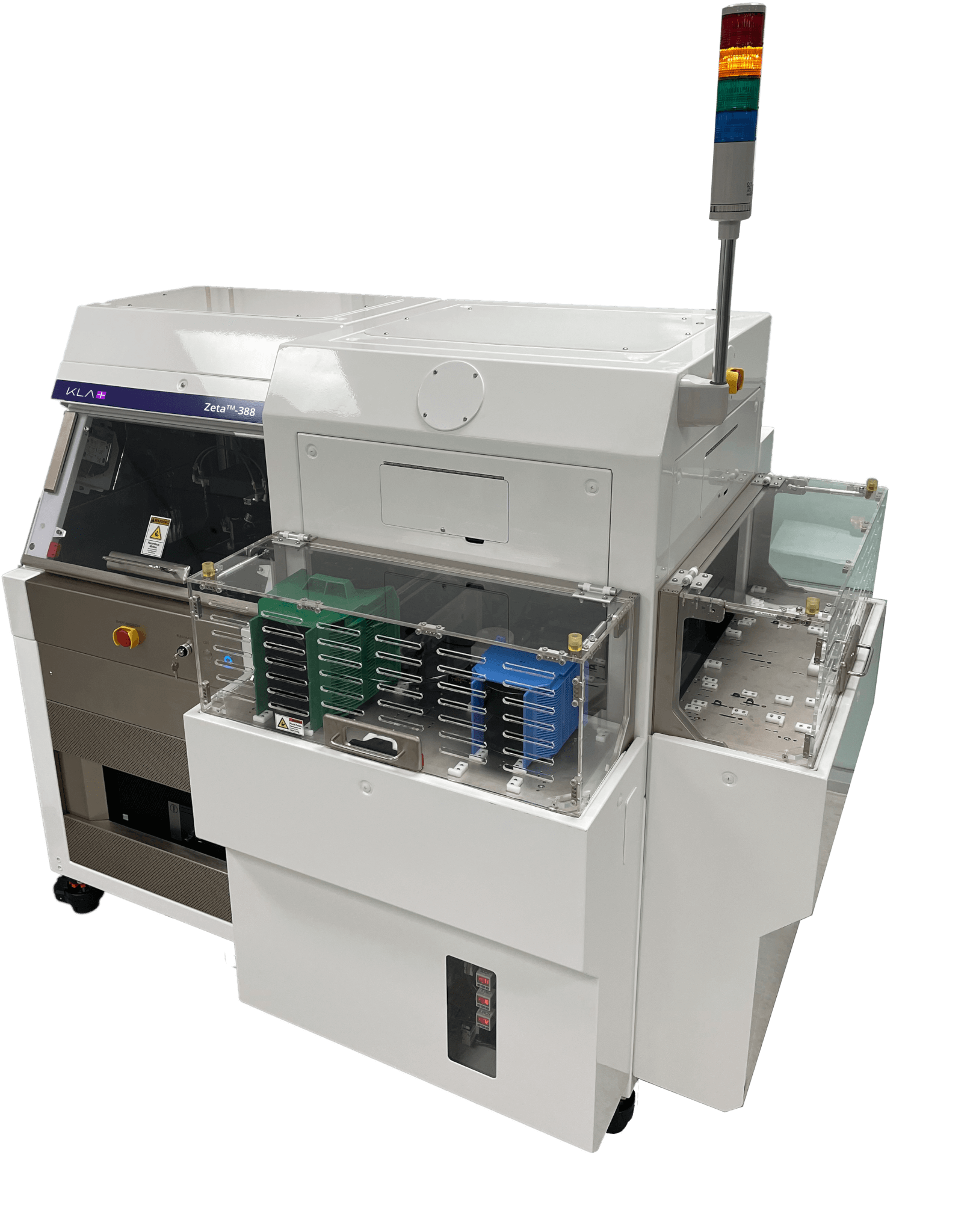
Zeta™-388 Optical Profiler
The Zeta-388 3D surface topography measurement system brings metrology automation to production by combining the Zeta-300 non-contact 3D optical profiler system with a cassette-to-cassette wafer handler, pattern recognition, automated data analysis and SECS/GEM to support production measurement requirements.
Frequently Asked Questions
-
What is an optical profiler?
An optical profiler is a non-contact surface metrology instrument that uses light-based measurement techniques to create a 3D map of a surface. Optical profilers are commonly used to measure surface topography, step height, roughness, film thickness, and surface defects.
-
How does an optical profiler work?
An optical profiler directs light onto a sample and analyzes the reflected light to determine surface height and reconstruct a 3D map of the surface. Most optical profilers use techniques such as white light interferometry (WLI), vertical scanning interferometry (VSI), structured illumination, phase shifting interferometry (PSI), confocal microscopy, or focus variation.
-
What is the difference between PSI and VSI?
Phase Shifting Interferometry (PSI) and Vertical Scanning Interferometry (VSI) are optical profiling techniques suited to different surface characteristics and measurement requirements.
PSI (Phase Shifting Interferometry)
- Best for smooth surfaces
- Extremely high vertical resolution
- Fast measurements
- Limited vertical range
VSI (Vertical Scanning Interferometry)
- Better for rougher surfaces
- Larger measurement range
- Suitable for step heights and surface texture characterization
-
What is the difference between a white light interferometer and a confocal profiler?
White light interferometry uses interference patterns from reflected light to determine surface height and can provide exceptional vertical resolution for a wide range of surface topography measurements. Confocal optical profiling uses focus-based optical sectioning to determine surface height and can be well suited to surfaces and structures that are challenging for interferometry. The best technique depends on factors such as surface roughness, slope, reflectivity, and feature geometry.
-
What can an optical profiler measure?
Optical profilers can measure and characterize a wide range of surface features and properties, including:
- Step height
- Surface roughness
- Etch depth
- Film thickness
- Flatness
- Bow and warp
- Particle dimensions
- Volume measurements
- Surface defects
- 3D topography
-
Can optical profilers measure rough surfaces?
Yes. Optical profilers can measure a wide range of rough and textured surfaces. Techniques such as VSI and Enhanced Roughness Mode are specifically designed to measure rough and highly textured surfaces. The appropriate measurement mode depends on factors such as surface roughness, reflectivity, slope, and the profiler being used.
-
Can optical profilers measure transparent films?
Yes. Many optical profilers can measure transparent films using specialized algorithms and optical models. Film thickness measurements are a common application.
-
What is the minimum step height an optical profiler can measure?
Modern interferometric optical profilers can measure nanometer-scale and even sub-nanometer surface features depending on the measurement mode and sample characteristics.
-
What is the maximum measurable step height an optical profiler can measure?
Maximum measurable step height depends on the system design, objective lens, and stage travel. Many modern optical profilers can measure structures ranging from nanometers to millimeters in height.
-
What are the advantages of optical profilometry compared to stylus profilometry?
Compared with contact-based stylus profilometry, optical profilometry can offer several advantages, including:
- Non-contact measurement
- Faster area measurements
- True 3D surface mapping
- No risk of scratching delicate samples
- High throughput for research and production environments
Stylus profilers are recommended for thin transparent films, adjacent dissimilar materials, very steep structures, or applications requiring direct physical tracing.
-
How do I choose the right optical profiler?
Choosing the right optical profiler depends on your measurement requirements, sample characteristics, and throughput needs. Key considerations include:
- Surface roughness scale/size
- Step height range
- Sample size
- Required throughput
- Vertical resolution requirements
- Material type
- Whether the sample is reflective, transparent, rough, smooth, or highly sloped
-
Which industries and applications use optical profilometry?
Optical profilers are widely used for surface metrology, process development, and quality control in:
- Semiconductor manufacturing
- MEMS
- Photonics and optics
- Advanced packaging
- Solar cells
- Medical devices
- Microfluidics
- Precision machining
- Additive manufacturing
- Academic research
-
Can optical profilers be used in production?
Yes. Optical profilers can be used in both R&D and production environments. Many systems support automated measurement routines, pass/fail analysis, defect inspection, wafer handling, and statistical process control for manufacturing environments.
-
How do I get started with KLA optical profilometry?
Fill out this inquiry form to get the process started, and one of our applications or sales representatives will contact you to discuss your applications requirements and answer any initial questions on pricing and lead times. A quote can be sent to you at this time, or you may wish to schedule a demo, either in-person or by sending samples for measurement. If a demo is completed, the report will be generated for you, after which you can decide how you would like to move forward.
-
What happens once I place an order?
Once an order is placed, your salesperson will keep you apprised of delivery schedule. Install and training is 1 day or less for the benchtop profilers, or longer for the automated systems. Some maintenance (such as calibration) can be performed by you. To order new or replacement step height standards, contact your sales representative. For questions that may arise as you are using the tool, our global Applications Team can provide assistance.
Looking for best-in-class stylus surface profilometers?
View MoreTechnical Literature
Browse application notes and technical papers from KLA Instruments Application Engineers and customers, covering a variety of use cases for KLA Instruments products.
Timeline of Innovation
The history of the optical profiler portfolio of KLA Instruments™ is a story of innovation from diverse origins. ADE launched the MicroXAM interferometer. Zeta™ Instruments developed ZDot™ and multi-mode optical profilers. Filmetrics® introduced novel, general-purpose white-light interferometers. These products came together into a diverse portfolio of optical profilometers, now unified under the KLA Instruments brand. Learn more about our rich history of innovation and how our tools continue to evolve to support your surface metrology requirements.
Receive the latest KLA Instruments news, papers, events, and more
Follow KLA Instruments
Follow KLA Instruments to engage with our experts and learn about our tool applications.
Learn how our products can help you.
Explore More Solutions

Instruments
For industry experts, academics and other innovators, KLA Instruments delivers trusted metrology and defect inspection solutions that provide measurements that enable the world’s breakthrough technologies.

Automated Metrology
KLA Instruments automated metrology instruments enable fab process control to quantify electrical properties, material deposited/removed, surface topography/roughness and critical dimensions. Automated metrology options include optical profilometry, stylus profilometry and film thickness mapping.
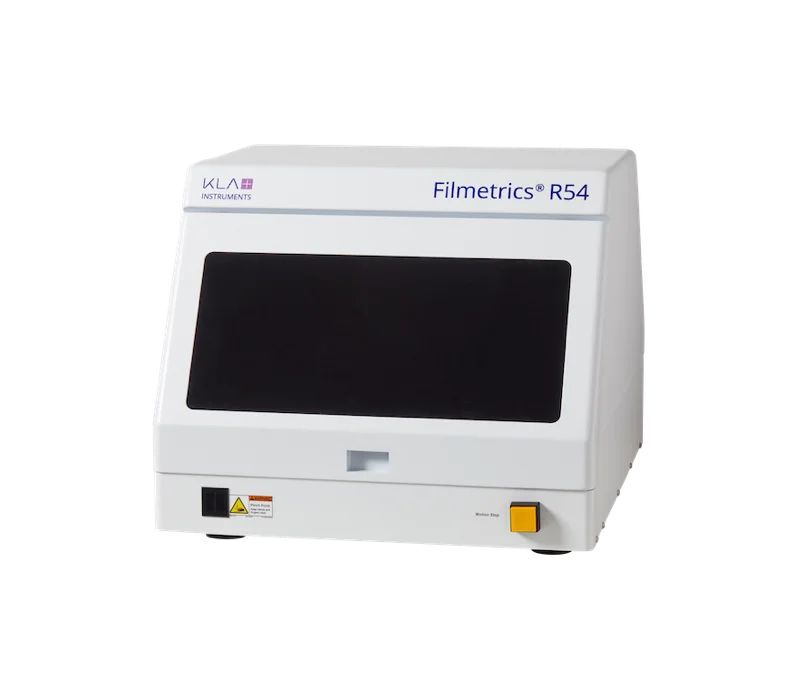
Filmetrics® Sheet Resistance Measurement Systems
The Filmetrics® benchtop and automated sheet resistance mapping instruments have been developed using decades of resistance measurement innovation and technical expertise. All Filmetrics models measure resist thickness and index by accurately modeling spectral reflectance.
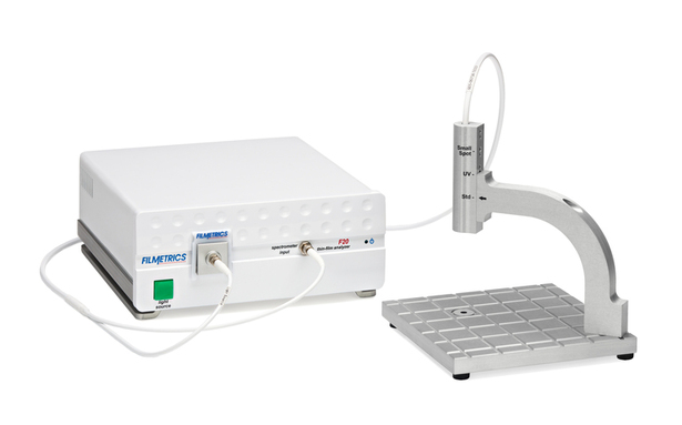
Filmetrics® Thin-Film Thickness Measurement Systems
The Filmetrics® thin-film reflectometers provide thickness and refractive index measurements of transparent films in seconds. These non-contact measuring instruments are available for both benchtop and production environments.
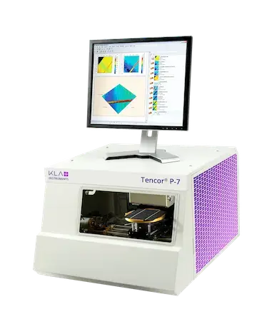
Stylus Profilers
The Alpha-Step®, Tencor® P-series and HRP® stylus profilometers enable high-precision, 2D and 3D surface metrology. The stylus profilers measure step height, roughness, bow and stress with industry-leading stability and reliability for your R&D and production metrology requirements.
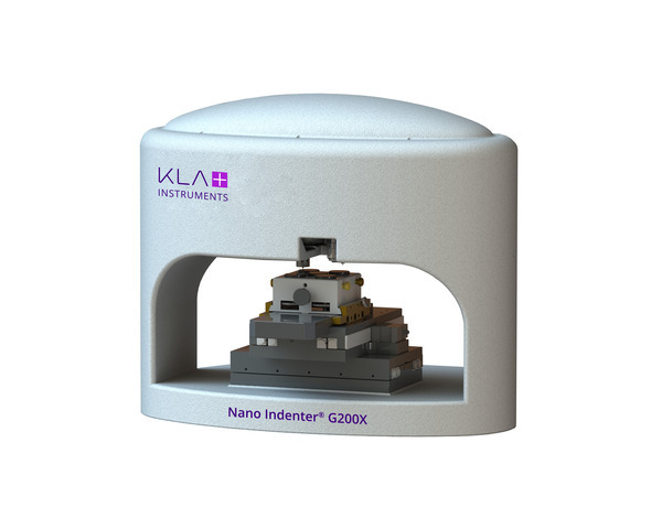
Nanoindenters
The KLA Instruments nanoindenter portfolio provides precise, reliable and repeatable nanoindentation and hardness testing to characterize static and dynamic mechanical properties of materials, under a wide range of test conditions.