
YAVNE, ISRAEL | ORBOTECH LTD. (NASDAQ: ORBK) today announced that SPTS Technologies, an Orbotech company and a supplier of advanced wafer processing solutions for the global semiconductor and related industries, has won an order for its Mosaic Plasma Dicing System from JCAP Corporation (Jiangyin Changdian Advanced Packaging Co., Ltd), a JCET company and leading Chinese advanced packaging services provider to global semiconductor companies. Orbotech's SPTS also announced that a recent analysis of MEMS microphones in the iPhone 7 Plus conducted by System Plus Consulting[1] confirmed that an ASIC device in the iPhone 7 Plus had been plasma diced.
Commenting on this recent order, Kevin Crofton, Corporate Vice President at Orbotech and President of SPTS Technologies, said: “JCAP selected Orbotech’s SPTS plasma dicing solution over competing options because the Mosaic system demonstrated superior results and offers lower cost of ownership. We were also selected for our inclusive approach and willingness to work alongside other suppliers in the back-end space to produce sustainable process flows.”
Mr. Crofton continued, “The Mosaic platform configured with the Rapier-300S is designed for handling 400mm framed wafers in a high volume manufacturing environment. It allows customers to offer industry-leading plasma dicing services that will meet the packaging needs of next generation devices. By adding plasma dicing to their service portfolio, customers can provide higher value packaging services and gain improved profitability in a highly cost sensitive industry.”
According to Amandine Pizzagalli, Technology & Market Analyst, at Yole Développement and author of the report entitled “Thin Wafer Processing and Dicing Equipment Market”[2], “Plasma dicing could reshape the dicing industry landscape by increasing the number of chips per wafer and thus reducing the cost of ownership of the dicing process. Driven by the rising demand for thinner wafers and stronger die, plasma dicing is positioned to become the only viable dicing option for next generation ultra small, ultra thin and fragile devices such as RFID, MEMS, and Power devices.”
Mr. Crofton added, “We have had continuous interest in the Mosaic plasma dicing solutions in our demo lab, and we continue to win business and expand our installed base. We see this as a real validation of our dicing platform. System Plus Consulting’s discovery of a plasma diced ASIC in the iPhone 7 Plus, which has been processed by our equipment, confirms industry acceptance and adoption of plasma dicing as a singulation method in the industry in high volume manufacturing.”
####
About Mosaic Plasma Dicing System
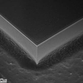
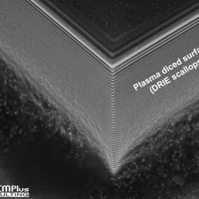
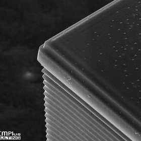
Orbotech's SPTS Mosaic™ plasma dicing system with the Rapier-300S overcomes many of the design limitations of conventional dicing methods, particularly for smaller, thinner, more fragile die, as well as offering the potential for significant increases in yield and throughput. The Rapier-300S is a silicon DRIE module, designed specifically for dicing of 300mm wafers mounted on 400mm frames and is available along with plasma dicing solutions for 150mm, 200mm and 300mm wafers. Unique aspects of SPTS’s plasma dicing technology include the use of SPTS’s patented Sentinel™ end-point detection and “bias pulsing” techniques to maximize die strength.
To learn more about SPTS’s Rapier-300S and Mosaic plasma dicing platform go to the Tech Insights section for articles on dice before grind (DBG) and dice after grind (DAG). Published papers and presentations can also be found in the Resources section.
[1] Knowles MEMS Microphones in iPhone 7 Reverse Costing Analysis, System Plus Consulting, October 2016
[2]Thin Wafer Processing and Dicing Equipment Market report, Yole Développement, May 2016
About Orbotech Ltd.
Orbotech Ltd. (NASDAQ:ORBK) is a global innovator of enabling technologies used in the manufacture of the world’s most sophisticated consumer and industrial products throughout the electronics and adjacent industries. Orbotech is a leading provider of yield enhancement and production solutions for electronics reading, writing and connecting, used by manufacturers of printed circuit boards, flat panel displays, advanced packaging, micro-electro-mechanical systems (MEMS), RF devices, power semiconductors, and other electronic components. Orbotech’s solutions include automated optical inspection and shaping, direct imaging, laser drilling, Inkjet printing, array test and repair, yield management, and etch and deposition wafer process solutions.
Today, virtually every electronic device in the world is produced using Orbotech systems. For more information, visit www.orbotech.com
ORBOTECH COMPANY CONTACTS:
Rami Rozen
Director of Investor Relations
Tel: +972-8-942-3582
Tally Kaplan Porat
Director of Corporate Marketing
Tel: +972-8-942-3603