
SAN FRANCISCO – Nano-electronics research center imec and SPTS Technologies, an Orbotech company (NASDAQ: ORBK) and supplier of advanced wafer processing solutions for the global semiconductor and related industries, announced today at SEMICON West that they are jointly developing a highly accurate, short cycle-time dry silicon removal and low temperature passivation solution for through-silicon via-middle processing and thinning of the top-wafer in wafer-to-wafer bonding.
Wafer backside processing is critical for 3D-IC wafer stacking. Today, through-silicon vias (TSV) formed using ‘via-middle’ processing, are typically exposed from the backside of 300mm device wafers by a combination of mechanical grinding and wet or dry etch processes. Dielectric layers are then deposited by plasma enhanced chemical vapor deposition (PECVD) to passivate and mechanically support the exposed TSVs prior to bump/RDL (redistribution) formation, followed by chip-to-wafer or wafer-to-wafer bonding.
To develop an industrially viable 3D-IC technology, the via reveal process requires a shorter cycle-time etching process. Additionally, due to accumulating non-uniformities coming from the TSV frontside etching, bonding and grinding processes, variations of a few microns may occur in residual silicon thickness above the via tips. Therefore, a highly selective process to thin TSV liners and smooth post-etch surfaces is essential to achieve the necessary precision and control within wafer uniformity.
Imec and SPTS are developing a dry etching solution that features in-situ end-point detection. This enables controlled and very precise processing. The process achieves the required TSV height while avoiding lengthy and multiple rework steps thus minimizing the overall cost per wafer. Our first results demonstrate that 1.57µm nail height can be controlled within 300nm range (see image below).
To follow the via reveal etch step, imec and SPTS will also work on PECVD dielectric passivation stacks, with SiO and SiN layers deposited at temperatures below 200°C. Films will be engineered to optimise device electrical performance and stress-managed to minimize warpage of the thin die after debonding,
The collaboration will use SPTS’s Versalis fxP system, a single-wafer cluster platform carrying both etch and dielectric deposition modules to be installed into imec’s 300mm packaging line in Q32015.
“Equipment suppliers are key in developing an integrated solution for the challenges of scaling technology into advanced nodes,” said An Steegen, senior vice president process technology at imec. “The collaboration with SPTS confirms imec’s direction to accelerate innovation for all our partners by closely interacting with suppliers at an early stage of development.”
“Imec plays a critical role in the long term development of the entire semiconductor value chain, from front to back-end,” said Kevin Crofton President of SPTS, and Corporate Vice President at Orbotech. “Their pre-competitive work supports the roadmaps of their core customers. Their remit dictates that they work with vendors and processes that are enabling for imec and their partners, and to be selected is a huge endorsement of our capabilities. We look forward to the results and milestones that we will achieve together.”
Imec’s research into 3D-IC includes key partners such as GLOBALFOUNDRIES, INTEL, Micron, Panasonic, Samsung, SK Hynix, Sony, and TSMC.
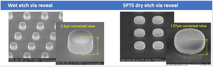
Top SEM view for wet and SPTS dry etch via reveal process
About imec
Imec performs world-leading research in nanoelectronics. Imec leverages its scientific knowledge with the innovative power of its global partnerships in ICT, healthcare and energy. Imec delivers industry-relevant technology solutions. In a unique high-tech environment, its international top talent is committed to providing the building blocks for a better life in a sustainable society. Imec is headquartered in Leuven, Belgium, and has offices in the Netherlands, Taiwan, USA, China, India and Japan. Its staff of about 2,200 people includes almost 700 industrial residents and guest researchers. In 2014, imec's revenue (P&L) totaled 363 million euro. Further information on imec can be found at www.imec.be. Stay up to date about what’s happening at imec with the monthly imec magazine, available for tablets and smartphones (as an app for iOS and Android), or via the website www.imec.be/imecmagazine
Imec is a registered trademark for the activities of IMEC International (a legal entity set up under Belgian law as a "stichting van openbaar nut”), imec Belgium (IMEC vzw supported by the Flemish Government), imec the Netherlands (Stichting IMEC Nederland, part of Holst Centre which is supported by the Dutch Government), imec Taiwan (IMEC Taiwan Co.)and imec China (IMEC Microelectronics (Shanghai) Co. Ltd.) and imec India (Imec India Private Limited).
About Orbotech
Orbotech Ltd. (NASDAQ:ORBK) is a global innovator of enabling technologies used in the manufacture of the world’s most sophisticated consumer and industrial products throughout the electronics and adjacent industries. The Company is a leading provider of yield enhancement and production solutions for electronics reading, writing and connecting, used by manufacturers of printed circuit boards, flat panel displays, advanced packaging, micro-electro-mechanical systems and other electronic components. Virtually every electronic device in the world is produced using Orbotech systems. For more information, visit http://www.orbotech.com/.
About SPTS Technologies
SPTS Technologies, an Orbotech company, designs, manufactures, sells, and supports etch, PVD and CVD awafer processing solutions for the MEMS, advanced packaging, LEDs, high speed RF on GaAs, and power management device markets. With manufacturing facilities in Newport, Wales and Allentown, Pennsylvania, the company operates across 19 countries in Europe, North America and Asia-Pacific. For more information, visit www.spts.com.
Contacts:
imec: Hanne Degans, Press officer and communications specialist, T: +32 16 28 17 69, Mobile : +32 486 06 51 75, Hanne.Degans@imec.be
SPTS: Destanie Clarke, Corporate Marketing Director, T:+44 7951 203278. destanie.clarke@orbotech.com
Orbotech: Anat Earon-Heilborn, Director of Investor Relations, Orbotech Ltd, T: +972 8 8942 3582
Ann Michael, Senior Corporate Marketing Communications Manager, Orbotech Ltd, T: +972 8 8942 3148