
Plasma Dicing
Stronger die - more die. High yield plasma dicing solutions based on industry leading Deep Reactive Ion Etch (DRIE) technology for dice-before-grind and dice-after-grind.
下載Wafer dicing is generally carried out using conventional blade technology. However this method has limitations which can be overcome by using dry plasma etching.
Blade cutting can cause die chipping or cracking leading to lower device yields. Also the necessary width of the blade removes valuable “real estate” from the wafer. Deep Reactive Ion Etching (DRIE) is a dry plasma process which can etch very narrow, deep vertical trenches into silicon (known as dicing “streets”) to separate individual die. Plasma dicing can either occur before grinding (DBG - Dice Before Grind) or after grinding (DAG – Dice After Grind).
There are many benefits when using plasma etch to separate die. SPTS’s DRIE technology allows designers to reduce dicing lane widths, remove damage exclusion zones and adopt flexible approaches to die shape and layout. All of which increases the number of die that can be arranged on a wafer.
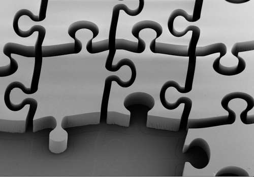
Test Structure illustrating potential for alternative die shapes
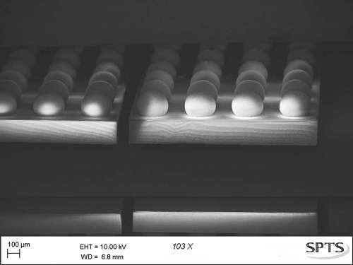
In the DBG approach, die are defined by partially etching the front side of a masked wafer up to a depth of approx 200µm. The wafer is then attached face-down to a dicing frame and the backside of the wafer ground away until singulation of the die occurs. Plasma dicing offers reduced cycle times and lower manufacturing costs when compared to conventional mechanical dicing. SPTS’s Mosaic™ Rapier-S DRIE systems provide 2 times greater throughputs than mechanical sawing, and have already been qualified at customer sites for this application.
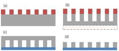
Schematic diagram illustrating Dicing Before Grind (DBG)
In DAG schemes, the thinned wafer is placed onto taped frames and the die are singulated by etching through to the tape. This method requires careful process control to prevent notching at the silicon-tape interface, and tape damage on exposure to the plasma. SPTS has a patented end-point and wafer protection solutions, capable of indicating the point at which the tape is reached, even for extremely low exposed silicon areas. This enables the process conditions to be adjusted during the short over-etch period used to complete the etch across the whole wafer. To further help eliminate notching, SPTS has a patented solution which uses RF pulsing, originally developed for etching MEMS devices on SOI wafers. This prevents the build-up of charge on the non-conducting tape and reduces deflection of ions into the sidewall. Investigations has proved that reduced notching equates to higher die strength. In fact, plasma etched die processed without this notch control are weaker than mechanically diced samples[1].
SPTS has worked with other suppliers to investigate and solve integration factors like dicing lane preparation, dicing tape selection[2], and post-dicing cleans[3] - Click here for more details. SPTS offers process demonstrations on customer sample wafers, in a dedicated plasma dicing lab in our UK headquarters. In addition to plasma dicing, we can also offer peripheral process steps including mounting on 296mm or 400mm frames, coating and laser grooving, post-dicing strip and clean and complementary metrology tools.
The SPTS system recommended for DAG is our Mosaic™ fxP Rapier, which is compatible with framed wafers up to 300mm.
The link you have selected is located on another server. Neither SPTS Ltd. nor any of its subsidiaries endorses this web site, its sponsor, or any of the information, policies, activities, products, or services offered on the site or by any advertiser on the site. By clicking on the OK button below, you agree and acknowledge the foregoing and will be directed to the selected site.