
Etch and Deposition Processes for MEMS
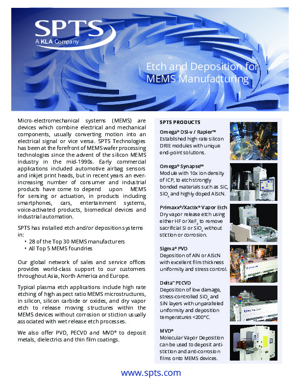
Overview of SPTS's etch and deposition processes used in MEMS manufacturing
Download
Overview of SPTS's etch and deposition processes used in MEMS manufacturing
Download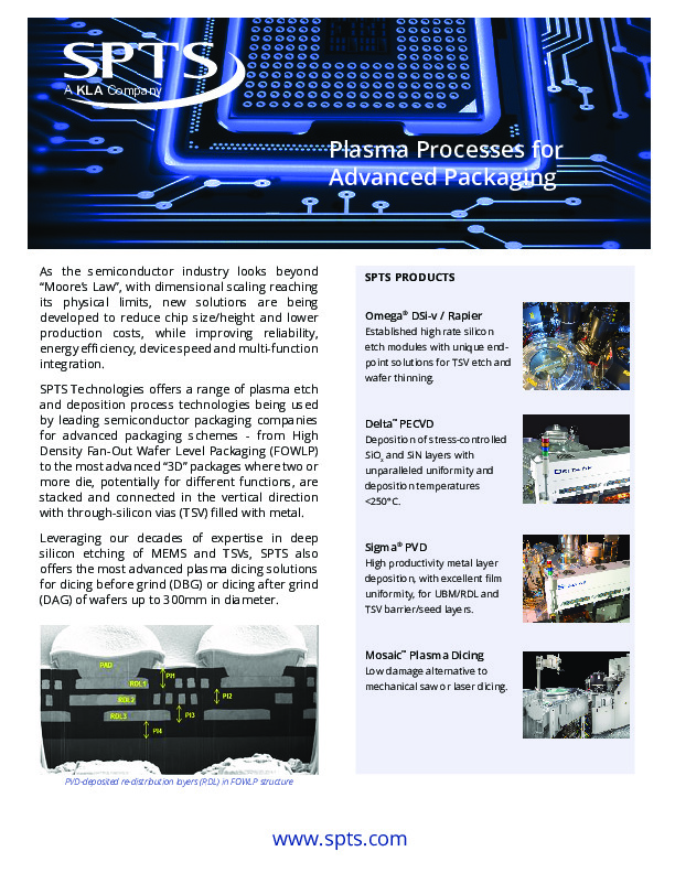
This datasheet gives an overview of the range of plasma etch and deposition process technologies being used by leading semiconductor packaging companies for advanced packaging schemes - from High Density FOWLP to the most advanced “3D” packages.
Download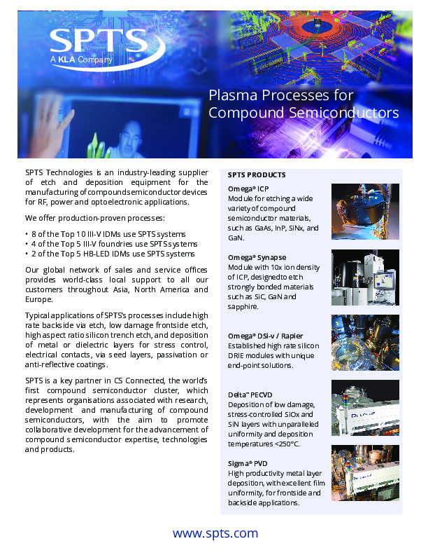
Overview of the plasma processing technologies which SPTS offers for a variety of compound semiconductor applications such as RF, power and photonic device manufacturing.
Download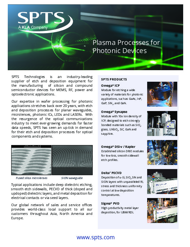
Download this datasheet giving an overview of SPTS's etch and deposition processes used to manufacture a range of photonic products such as LEDS, optical waveguides, VCSELs and lasers.
Download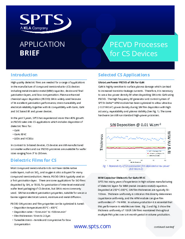
This SPTS' PECVD processes for deposition of SiN onto GaN and GaAs in RF, power, and photonic applications.
Download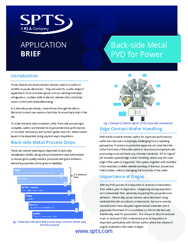
This Application Brief discusses the back-side metallization process for power device manufacturing, and the features of SPTS’s Sigma® fxp which offer reliable wafer handling, effective degas and pre-clean options, film stress control and higher throughputs.
Download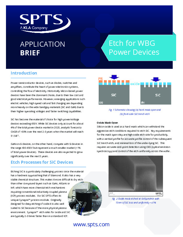
This Application Brief describes SPTS etch processes for SiC and GaN-on-Si power devices, using our ICP and Synapse etch modules
Download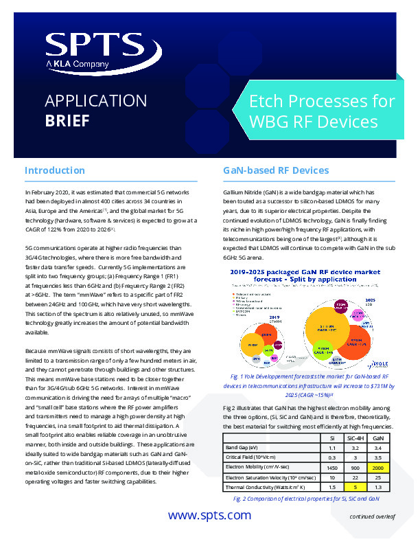
This Application Brief describes the reasons GaN is often selected for 5G applications, and SPTS's back-side SiC via and GaN etch processes used in the manufacturing of GaN-on-SiC RF devices.
Download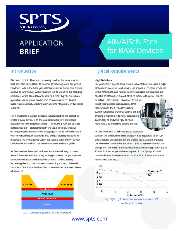
In this Application Brief we give an overview of the benefits of the Synapse module for etching AlN and AlScN for BAW device manufacturing, in terms of high etch rate, sidewall angle and end-point control
Download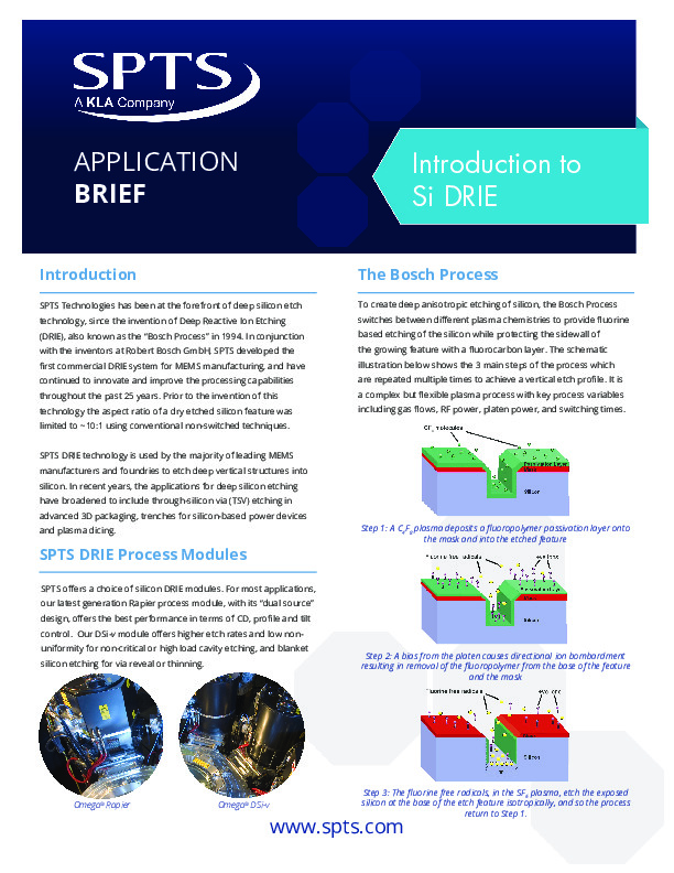
Brief introduction to silicon DRIE (The Bosch Process) and its application within MEMS, Advanced Packaging and Power Device manufacturing.
Download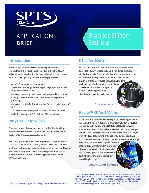
Download this datasheet explaining how dry blanket Si etching exhibits better control over the etch rate and uniformity, when compared to wet chemical approaches.
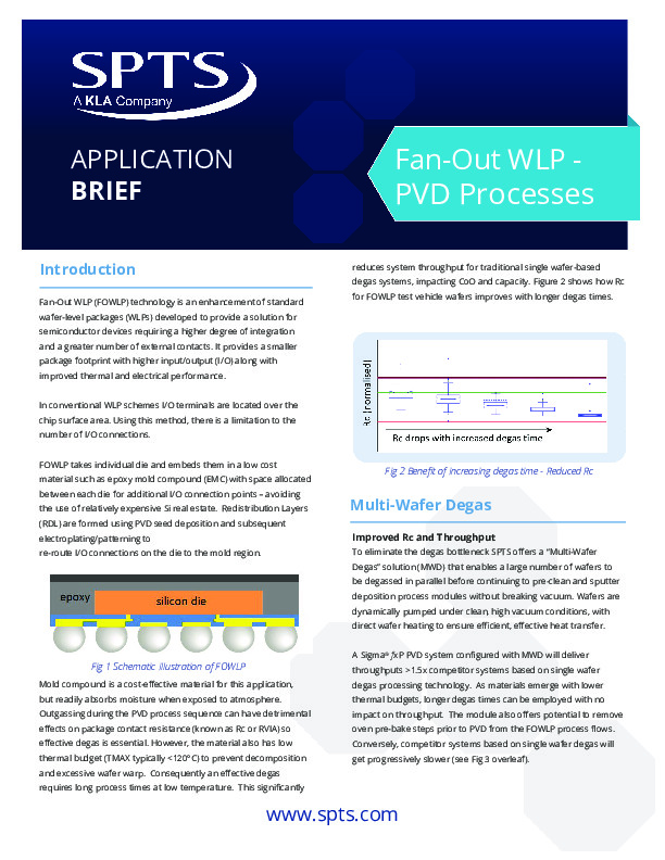
Download this datasheet describing how fan-out wafer-level packaging (FOWLP) technology provides higher integration levels and a greater number of external contacts.
Download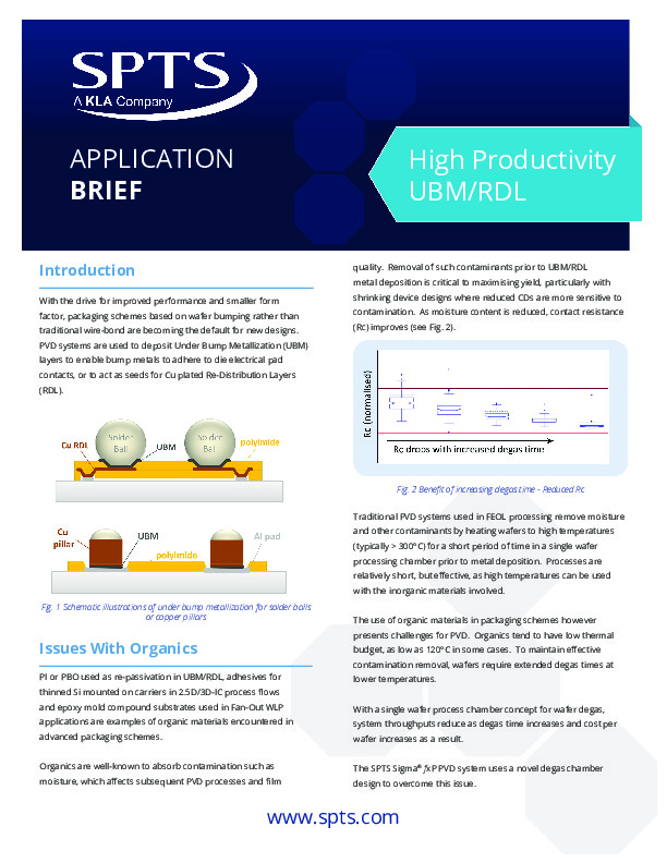
Download this datasheet describing PVD solutions to deposit Under Bump Metallization (UBM) layers, to enable bump metals to adhere to die electrical pad contacts, or to act as seeds for Cu plated Re-Distribution Layers (RDL).
Download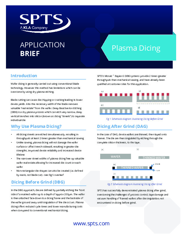
Stronger die - more die. High yield plasma dicing solutions based on industry leading Deep Reactive Ion Etch (DRIE) technology for dice-before-grind and dice-after-grind.
Download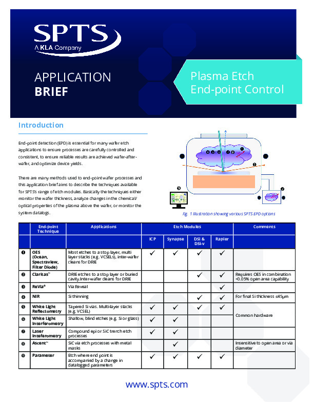
End-point detection (EPD) is essential for many wafer etch applications to ensure processes are carefully controlled and consistent.
Download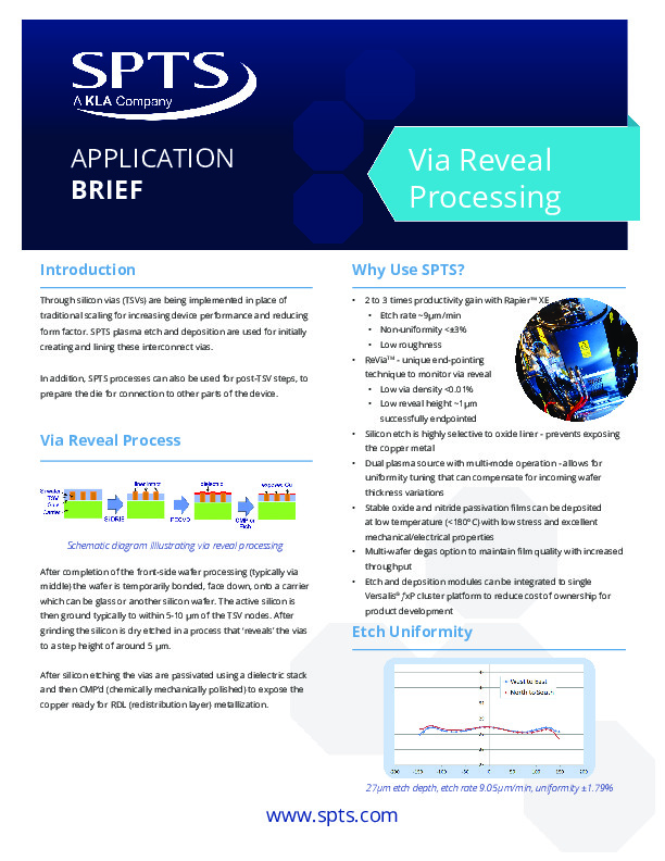
High productivity plasma etch processes with unique end-point detection used for post-TSV steps, to prepare the die for connection to other parts of the device.
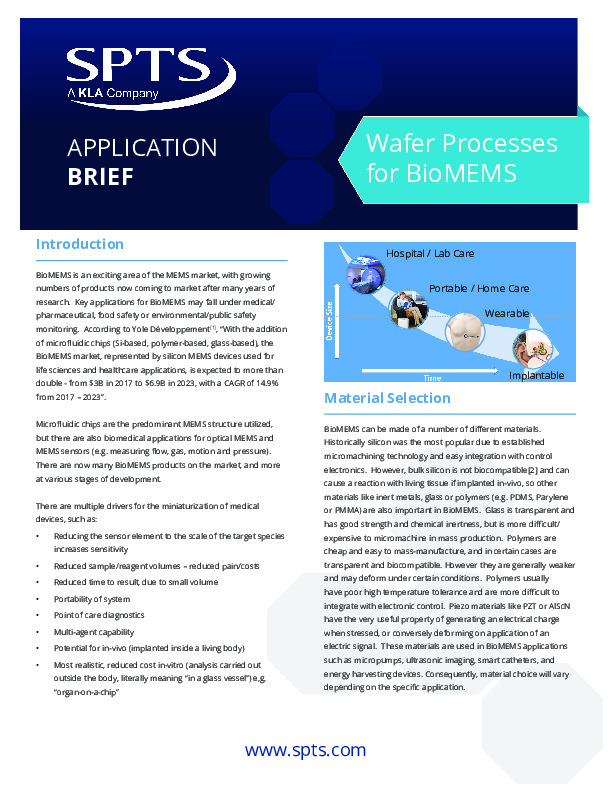
BioMEMS is an exciting area of the MEMS market, and SPTS offers a range of wafer processes which enable development and commercial manufacturing of BioMEMS
Download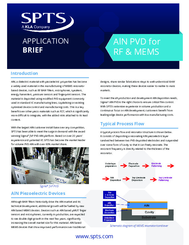
Piezoelectric properties of AlN to convert mechanical strain into an electric signal, or vice versa is being exploited in devices such as RF filters and a growing number of MEMS.
Download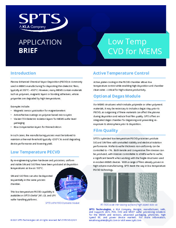
Low temp Plasma Enhanced Chemical Vapor Deposition (PECVD) solutions for depositing uniform and stable SiN and SiO films for MEMS devices at temperatures <200°C.
Download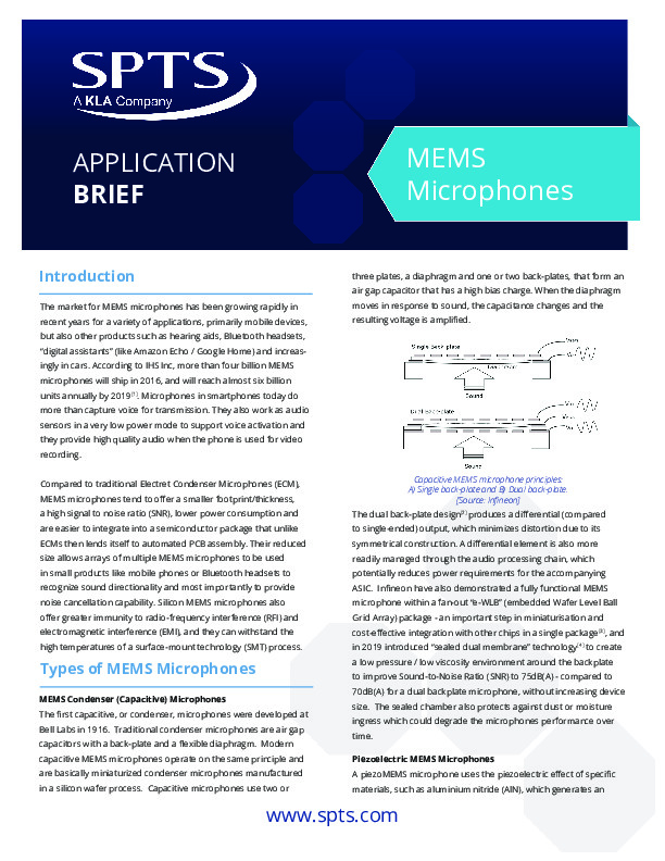
MEMS microphones have been growing rapidly in recent years for a variety of applications, primarily mobile devices, but also other products such as hearing aids, Bluetooth headsets, and “digital assistants”.
Download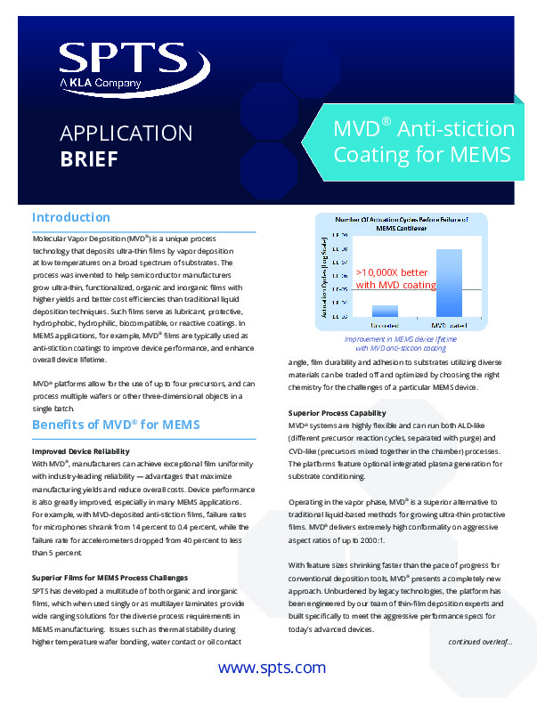
Molecular Vapor Deposition (MVD®) is a unique process technology that deposits ultra-thin films by vapor deposition at low temperatures on a broad spectrum of substrates.
Download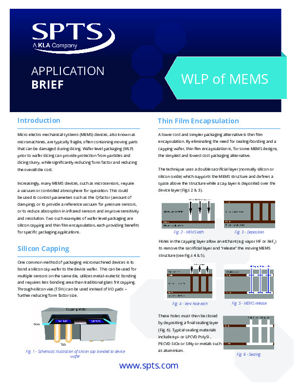
Wafer level packaging (WLP) prior to wafer dicing of MEMS devices can provide protection from particles and dicing slurry, while significantly reducing form factor and reducing the overall die cost.
Download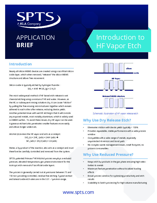
HF etching is a dry vapor (plasma-less) etch process to remove sacrificial oxide layers, primarily used to release silicon MEMS structures.
Download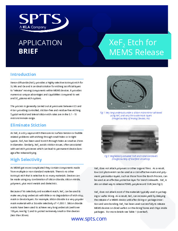
XeF2 vapor etching is a highly selective isotropic etch for removing sacrificial layers of Si, Mo or Ge to release MEMS miccrostructures.
Download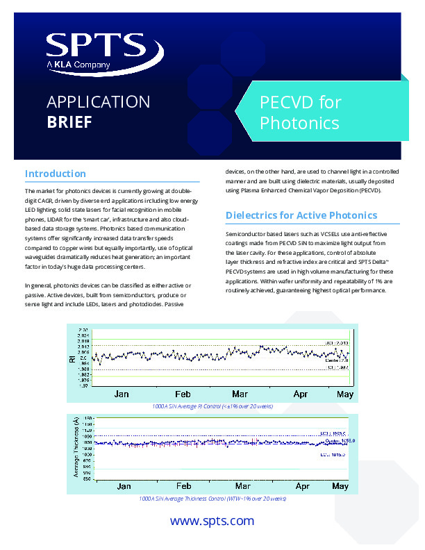
Download this datasheet illustrating how SPTS's PECVD processes can be used for depositing dielectrics for a number of photonic applications, such as thick doped/undoped films for optical waveguides or anti-reflective coating for VCSELs.
Download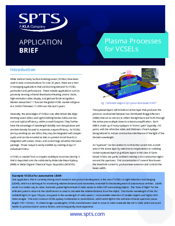
New applications for VCSELs include proximity sensing for automotives and gesture/face recognition for consumer products and SPTS offers a range of processes for VCSEL manufacturing including ICP etch, PVD, and PECVD.
Download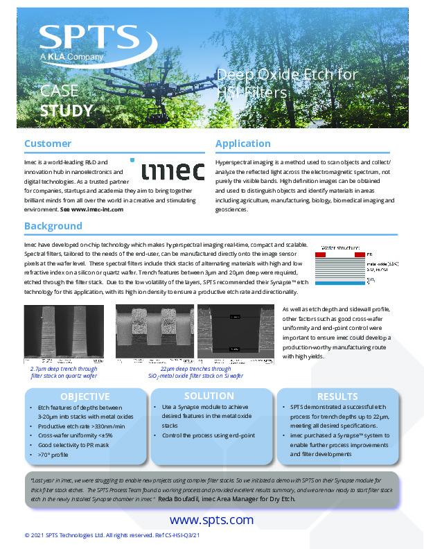
Case study showing how SPTS's Synapse etch module enabled the successful manufacturing of SiO2-metal oxide filter stacks, for use in hyperspectral imaging cameras
Download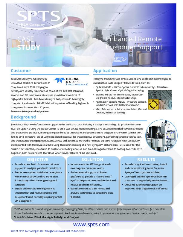
During COVID-19, SPTS implemented a remote support solution to enable the commissioning of a new etch system at Teledyne Micralyne when SPTS engineers could not be on-site.
Download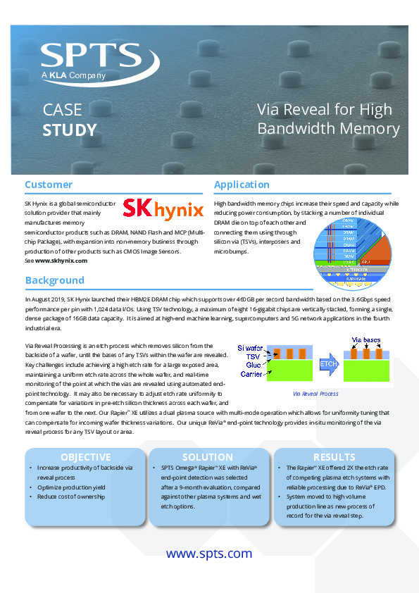
SPTS worked with SK Hynix to increase productivity of their backside via reveal process used in high bandwidth memory chip manufacturing - Optimizing production yield and reducing cost of ownership
Download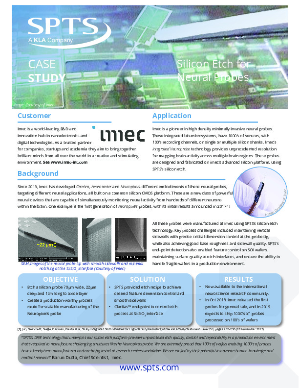
Download this Case Study illustrating how SPTS's Si DRIE technology is used by imec for manufacturing neural probes for mapping brain activity.
Download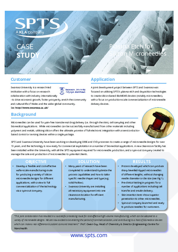
Illustrates the results of a joint development project between SPTS and University of Swansea to create a process for volume production of silicon microneedles for biomedical applications.
Download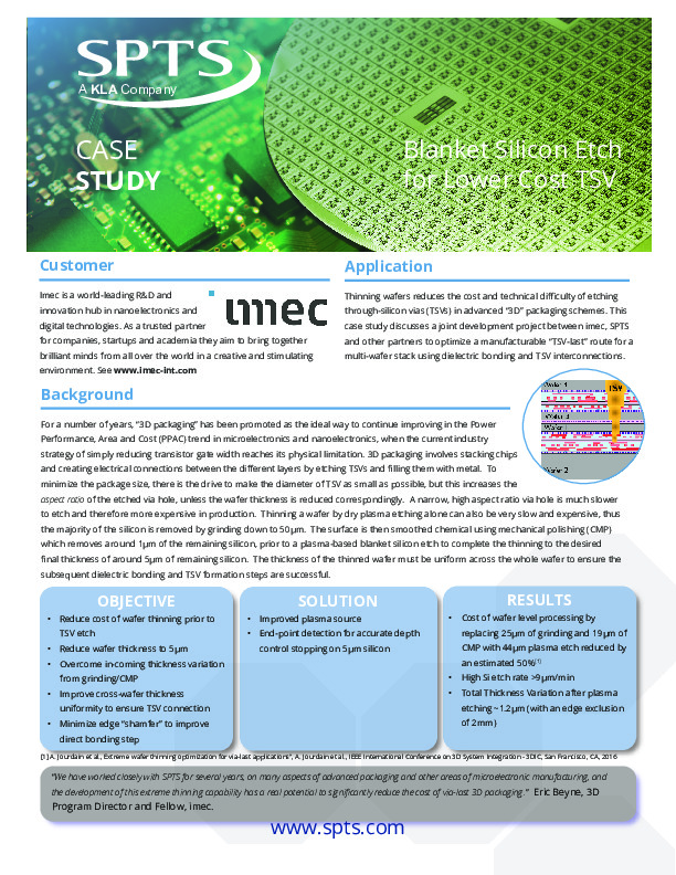
Discusses the introduction of blanket silicon etching to replace CMP, as part of a joint development project with imec to optimize a manufacturable "TSV-last" route for a multi-wafer stack.
Download
Describes how SPTS worked with Skyworks to significantly improve Mean Time Before Clean (MTBC) for a SiN etch step, used in the manufacturing of their GaAs RF devices.
DownloadThe link you have selected is located on another server. Neither SPTS Ltd. nor any of its subsidiaries endorses this web site, its sponsor, or any of the information, policies, activities, products, or services offered on the site or by any advertiser on the site. By clicking on the OK button below, you agree and acknowledge the foregoing and will be directed to the selected site.