
Plasma Dicing
Stronger die - more die. High yield plasma dicing solutions based on industry leading Deep Reactive Ion Etch (DRIE) technology for dice-before-grind and dice-after-grind.
下載The potential benefits of plasma dicing, illustrated in Fig 1, have been well-documented [1-4], and the approach is being increasingly employed for high volume products. SPTS is helping a growing number of device manufacturers to integrate this new technology into existing manufacturing schemes.
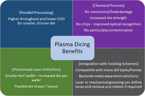
Fig 1 Potential Benefits of Plasma Dicing
In 2015, we shipped our first Mosaic™ plasma dicing system for 200mm silicon wafers on frames, and followed that with Rapier-300S process modules for 300mm wafers on 400mm frames. Recently, we have also demonstrated high rate plasma dicing of GaAs wafers. To enable the growing number of interested customers to investigate the benefits of plasma dicing, we have established a Plasma Dicing Demo Lab inside our Newport, UK facility, equipped with tape mounting, coating/LASER grooving, post-dicing strip/clean capability and a full suite of metrology tools alongside the Mosaic™ plasma dicing systems themselves.
To solve the new challenges posed by the introduction of a plasma etch singulation, SPTS has worked closely with other backend partners. To show the benefit of our inclusive approach, two examples of such collaborative work are detailed below:
Through demonstration work with various customers, we have gained experience of many industry-standard dicing tapes and generated a significant knowledge base of suitable tape options. For example, during a recent detailed study in conjunction with Lintec[5], it was found that polyolefin (PO) tapes performed better than PVC tapes. With a hard adhesive, and low-to-medium adhesive strength, PO tapes are the optimal choice with the lowest out-gassing rate and are least likely to declamp within aggressive (high etch rate) plasma etch conditions. In addition, die pick-up force measurements from the selected PO tapes, after plasma dicing in the Rapier-S process module, indicate the pick-up force on plasma-singulated die to be comparable with those diced in more traditional ways.
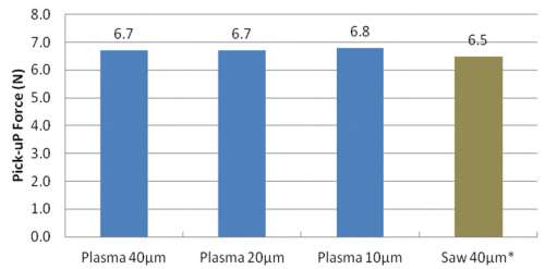
Fig. 2 Pick-Up Force measurements for 10x10mm die from a medium adhesion PO UV tape showing no significant effect on tape adhesion following plasma dicing for 3 different dicing lane widths, compared to saw dicing.
To download the full technical paper, published for EPTC2018, click here.
The plasma dicing process uses a fluorinated chemistry [2] that can leave behind fluorine (F) based residues on exposed surfaces. This could include solder bumps or bondpads.
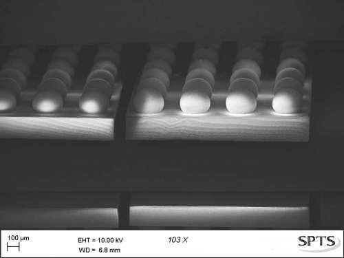
Fig 3 Plasma diced die containing solder balls
It is suggested that the presence of fluorine can lead to an increase in resistivity, contact failure or long-term reliability of wirebond connections. On the other hand, the presence of F may actually improve solderability with a thin layer of SnF2 promoting fresh solder from within the bump to the surface. One way of preventing this from occurring at all is to adopt an integration scheme which coats the exposed surfaces, maintaining a barrier shielding them from fluorine. Where coating is not feasible, there are ways to remove the fluorine after singulation. SPTS and Versum Materials have been testing various wet clean formulations to remove residual fluorine from the surface, potentially removing the need for a dry strip. All tested processes are compatible with tapes and adhesives. Process conditions were optimized for the most promising formulations and negligible (<0.5wt%) fluorine levels were found after treatment. This is comparable to samples that were not exposed to plasma dicing. The effects of the different wet clean processes on the dicing tape were then compared. Generally, the process temperature of the wet clean was found to be the most important factor. If the temperature was too high, the dicing tape could deform and result in possible die loss. To see the full results, presented at SEMICON Europa 2018[6], click here.
If you have a potential application for plasma dicing and want to discuss any aspect of the process capability and integration into your existing manufacturing route, please contact us now
References
[1] R. Barnett et al, “A New Plasma Source for Next Generation MEMS Deep Si Etching”, Proc. of IEEE 60th Electronic Components and Technology Conference, Las Vegas, NV, June 2010, pp.1056-1059
[2] R. Barnett et al "Considerations and Benefits of Plasma Etch Based Wafer Dicing" Proc. of 2013 IEEE 15th Electronics Packaging Technology Conference, Singapore, pp.569-574
[3] R. Barnett “Plasma Dicing 300mm Framed Wafers — Analysis of Improvement in Die Strength and Cost Benefits for Thin Die Singulation” Proc of 2017 IEEE 67th Electronic Components and Technology Conference Orlando, FL, June 2017, pp.343-349
[4] Thin Wafer Processing and Dicing Equipment Market Report, Yole Développement, May 2016
[5] Fulton, S. et al “Dicing Tape Performance in a Plasma Dicing Environment” Presented at 20th Electronics Packaging Technology Conference, Singapore, Dec 2018.
[6] Hopkins, J. et al “Optimising Surface Chemistry After Plasma Dicing” Presented at SEMICON Europa 2018
The link you have selected is located on another server. Neither SPTS Ltd. nor any of its subsidiaries endorses this web site, its sponsor, or any of the information, policies, activities, products, or services offered on the site or by any advertiser on the site. By clicking on the OK button below, you agree and acknowledge the foregoing and will be directed to the selected site.