
PECVD Processes for Compound Semiconductor Devices
This SPTS' PECVD processes for deposition of SiN onto GaN and GaAs in RF, power, and photonic applications.
下载High quality dielectric films are needed for a range of applications in the manufacture of compound semiconductor (CS) devices including metal-insulator-metal (MIM) capacitor, device and final passivation layers, and bow compensation. Plasma enhanced chemical vapor deposition (PECVD) SiN is widely used because of its excellent passivation performance, stress tuneability and electrical reliability together with its compatibility with GaAs, GaN and SiC based RF and power devices.
In the past 5 years, SPTS has experienced more than 40% growth in PECVD sales into CS applications which includes deposition of dielectric films for:
In contrast to Si-based devices, CS devices are still manufactured on smaller wafers and our PECVD processes are available for wafer sizes ranging from 3” to 200mm.
Most compound semiconductors do not have stable native oxide layers, such as SiO2, and oxygen is also a dopant for many compound semiconductors. Hence, PECVD SiN is typically used as a first passivation layer. There are some applications for SiO films deposited by SiH4 or TEOS, for passivation of inter-level metal and wafer level packaging of CS devices, but SiN is more commonly used. SiN has excellent passivation properties, suitable for use as a barrier against electrical current, moisture and metal diffusion.
PECVD SiN process and film properties can be optimized & tuned:
Ultra-Low Power PECVD of SiN for GaN
GaN is highly sensitive to surface plasma damage which can lead to increased transistor leakage currents. Therefore, it is necessary to use a low power density RF when depositing SiN onto GaN using PECVD. The high frequency RF generator and control system of SPTS’s Delta™ APM module has been optimized to allow ultra-low (~0.01W/cm2) power density during SiN film deposition with high accuracy, repeatability and plasma stability. The same hardware can still run standard high-power processes.
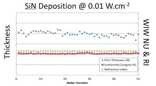
Fig 1 Repeatability of SiN passivation film deposited at low power (0.01W.cm-2)
MIM Capacitor Dielectric for GaAs RF-IC
SPTS has many years of experience in high volume manufacturing of dielectric layers for MIM (metal- insulator-metal) capacitors. Deposited at 250°C – 300°C, SiN film thicknesses are typically 50nm – 100nm. Thickness uniformity is critical as this directly determines capacitance uniformity, and the APM module can give film uniformities of ~1% WIW. In volume production it is essential that this performance is reliable over time. The graphs below show the thickness uniformity of 1000Å SiN films maintained throughout multiple PM cycles over a 4-month period in volume production.
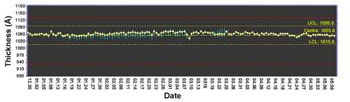
Fig 2 Average thickness for 1000 Å SiN films over 4 months, in production
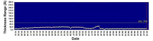
Fig 3 WIW Thickness Range for 1000 Å SiN films over 4 months in production
The electrical performance and long-term reliability of the dielectric films is also very important, and SPTS’s SiN films have a proven performance with voltage breakdown ~ 10MV.cm-1 and resistance to time dependent dielectric breakdown (TDDB).
Anti-Reflective Coating for GaAs-based VCSELs
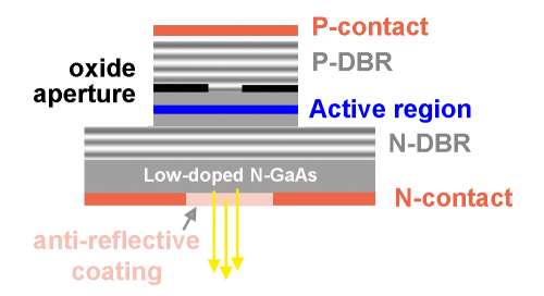
Fig 4 Schematic diagram of VCSEL structure with anti-reflective coating on the back side of the GaAs substrate
SiN can also be used as an anti-reflective coating which improves the efficiency of VCSELs. Control of thickness and refractive index are paramount for best optical performance. SiN can also be useful as a stress compensation layer minimizing wafer bow for thinned substrates. Applied to the back side of the GaAs wafer, it is important to avoid mechanical damage to the active layers on the frontside. SPTS’s Delta™ PECVD offers an “edge-contact” option with a modified platen and pin-lift which eliminate the need for expensive frontside protection layer.
There are a number of features of the Delta APM module which are important to CS applications (as well as standard silicon) namely:
The Delta™ fxP PECVD is an excellent choice for deposition of dielectrics for a wide range of compound semiconductor applications. It offers a flexible solution that combines excellent dielectric film properties across a wide range of deposition temperatures, combined with high throughput and repeatable processing performance in high volume production
The link you have selected is located on another server. Neither SPTS Ltd. nor any of its subsidiaries endorses this web site, its sponsor, or any of the information, policies, activities, products, or services offered on the site or by any advertiser on the site. By clicking on the OK button below, you agree and acknowledge the foregoing and will be directed to the selected site.