PECVD for Photonics
Introduction
The market for photonics devices is currently growing at double-digit CAGR, driven by diverse end applications including low energy LED lighting, solid state lasers for facial recognition in mobile phones, LIDAR for the ‘smart car’, infrastructure and also cloud-based data storage systems. Photonics based communication systems offer significantly increased data transfer speeds compared to copper wires but equally importantly, use of optical waveguides dramatically reduces heat generation; an important factor in today’s huge data processing centers.
In general, photonics devices can be classified as either active or passive. Active devices, built from semiconductors, produce or sense light and include LEDs, lasers and photodiodes. Passive devices, on the other hand, are used to channel light in a controlled manner and are built using dielectric materials, usually deposited using Plasma Enhanced Chemical Vapor Deposition (PECVD).
Dielectrics for Active Photonics
Semiconductor based lasers such as VCSELs use anti-reflective coatings made from PECVD SiN to maximize light output from the laser cavity. For these applications, control of absolute layer thickness and refractive index are critical and SPTS Delta® PECVD systems are used in high volume manufacturing for these applications. Within wafer uniformity and repeatability of 1% are routinely achieved, guaranteeing highest optical performance.
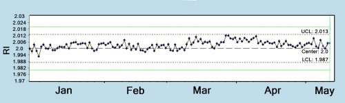
1000Å SiN Average RI Control (<±1% pver 20 weeks)
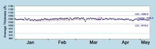
1000Å SiN Average Thickness Control (WTW~1% over 20 weeks)
Planar Waveguides
The planar waveguide market boomed in the 1990’s, driven by the widespread installation of infrastructure for fibre-optic broadband. Traditional planar waveguide devices are simple in concept: a PECVD silica core is doped with germanium (Ge) to increase the refractive index above that of SiO2. The doping is achieved by adding GeH4 gas to a standard PECVD SiO and adjusting the flows to give the required refractive index.
A second cladding layer of lower refractive index is deposited over the Ge-doped SiO core; usually PECVD silica doped with boron and phosphorus (Boro-Phospho-Silicate Glass or BPSG). The doping in this layer serves to reduce the reflow temperature of the glass when heated and allows the cladding to coat the core without voids or seams and with low stress. Wafers are typically annealed in a tube furnace at over 1000°C and the annealed, reflowed film is highly homogeneous which improves optical performance as the refractive index non-uniformity is reduced below that of the as-deposited film. The resultant structure provides a refractive index contrast between core and cladding, which serves to constrain light signals within the core through total internal reflection.
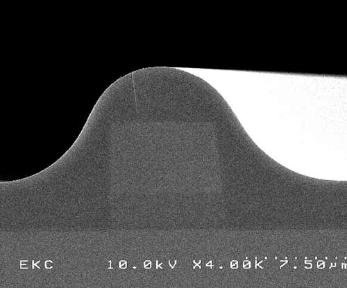
Silica waveguide with Ge-doped core and BPSG cladding
Next Generation Waveguides
While traditional doped silica waveguide devices still enjoy widespread use, the industry is constantly looking for ways to improve performance by reducing optical loss (attenuation). Optical loss in PECVD dielectrics is ultimately limited by the hydrogen content of the film, an unavoidable byproduct of the precursor gases used during the CVD reactions. Low loss waveguides can be produced without the need for silica doping. Instead, the required refractive index contrast between layers is obtained by process tuning and H content is minimised by optimal choice of precursor gases. By doing this, PECVD waveguides with optical loss <0.2dB/cm have been produced without the need for doping or high temperature anneal steps.
For automotive and facial recognition sensing, infrared wavelengths are used. At longer wavelengths, silica becomes too lossy for practical use and so other materials must be introduced. Silicon performs well as an infrared waveguide in both single crystal and amorphous forms. Amorphous silicon is readily deposited using PECVD at temperatures below 400°C using simple precursor mixes and such films are now being used for advanced infrared-based waveguide devices.
Delta™ PECVD for Waveguides
Dielectric films used in waveguides are relatively thick (≥5µm) and so stress must be minimized to prevent excessive substrate bow which will adversely affect subsequent lithography steps and can also cause unacceptable refractive index variation. Through hardware and process optimization, Delta™ PECVD systems can produce thick dielectric films with stress below 20 MPa, refractive index tuned across a suitably wide range and measured optical loss of ≤0.2dB/cm.
To maximize PECVD system productivity, both high deposition rates and high chamber cleaning rates are needed. Deposition rates of 1µm/min or more are readily achievable in Delta™ fxP systems and we have recently introduced a unique chamber cleaning configuration which enhances the cleaning rates obtained from conventional Remote Plasma Source (RPS) technology. Using the new RPS cleaning technology, industry leading productivity for thick waveguide dielectric films is realized.
For more information on SPTS process solutions for waveguides and other photonic applications, please contact your local SPTS Sales Office.
