
AlN PVD for RF-IC & MEMS
Piezoelectric properties of AlN to convert mechanical strain into an electric signal, or vice versa is being exploited in devices such as RF filters and a growing number of MEMS.
下载Aluminum Nitride (AlN) is a rare example of a ceramic material that combines high thermal conductivity with high electrical resistivity. Some describe it as a “miracle material” and it has a multitude of uses in various industries, such as molten materials handling, optoelectronics, heat sinks, microwave device packaging, and high power electronics.
Of most interest to the electronics industry is the piezoelectric properties of AlN; its ability to convert mechanical strain into an electric signal, or vice versa. This property is exploited in devices such as RF filters, produced in high volume for mobile communications applications, and a growing number of Micro Electro Mechanical Systems (MEMS).
Other piezoelectric materials include lead zirconium tantalite (PZT), lithium niobate, lithium tantalate and quartz. However, some of these materials are difficult to manufacture and PZT is a contaminant for standard CMOS IC processing. In contrast, AlN is CMOS-friendly and can be easily deposited in our Sigma® fxP PVD system by sputtering pure Al material in a N2/Ar plasma to form AlN on the surface of a wafer. In recent years, researchers have discovered that the piezoelectric properties of AlN can be significantly improved by the addition of scandium into the material. AlScN can also be successfully deposited with the Sigma® fxP, which has unique hardware options to address the issues which are introduced with increasing Sc content. Metal targets with up to 40at.%Sc are now available and being used to develop the next generation of BAW RF filters and piezoMEMS.
RF Filters
RF filters are devices which perform signal processing functions in wireless applications, including cell phones, GPS, Wi-Fi and Bluetooth, to remove unwanted frequency components from the signal, to enhance wanted ones, or both. With millions of communication devices operating at closely packed frequencies, effective filtering and signal optimization is crucial.
For many years, surface acoustic wave (SAW) filters offered good performance for low cost. SAW filters, however, have limitations. Above about 1 GHz, their selectivity declines and they also are notoriously sensitive to temperature changes. This led to the introduction of temperature-compensated (TC-SAW) filters, and then a move towards bulk acoustic wave (BAW) filters which perform much better at frequencies above 1.5GHz. BAW filters also have the attractive characteristic of decreasing size at higher frequencies, which makes them ideal for the most demanding 3G and 4G mobile applications. BAW filters are also far less sensitive to temperature variation, and have low insertion losses (i.e. loss of signal power due to insertion of the device) leading to longer cell phone battery life.
AlN is the piezoelectric material of choice for modern BAW devices, because it provides the best balance of performance, CMOS compatibility, manufacturability and reliability[1].
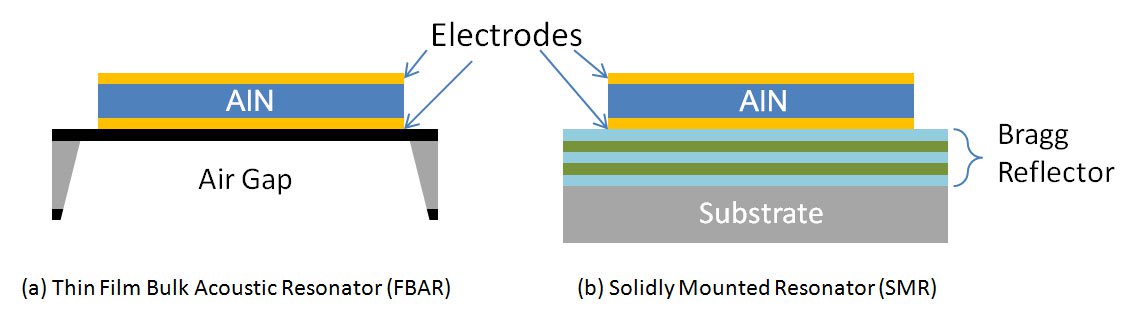 To make a BAW filter, a piezoelectric AlN layer is sandwiched between two PVD-deposited metallic electrodes (e.g. Mo, W, AlCu) and either suspended over a cavity etched into the substrate (i.e FBAR in Fig (a) above) or deposited onto a Bragg Reflector stack (SMR in Fig (b)). The cavity and stack are alternative methods to reflect both longitudinal and shear[2] acoustic waves, necessary to avoid losses from the substrate and improve the resonator’s “Quality” or “Q” factor.
To filter a signal a BAW device must resonate at a specified frequency. This frequency and its bandwidth depend upon the thickness and Q factor of the AlN film. To obtain the best performance from a BAW device the PVD process needs to deposit AlN with:
MEMS
There are a growing number of MEMS devices which use the same piezoelectric effect to convert mechanical strain or stress into a signal, such as microphones, energy harvesters, and ultrasonic transducers (e.g. fingerprint sensors). PiezoMEMS devices are more sensitive than traditional capacitive MEMS sensors and consume far less power, so are very relevant to the wearable device market, and will be an enabling technology in the IoT revolution. PiezoMEMS product announcements have started to appear such as Vesper’s microphone, and Invensense’s fingerprint sensor. We expect to see such enabling devices appear in marquee smartphones within the next two years.
[1] “Bulk Acoustic Wave Devices – Why, How, and Where They are Going” S. Mahon et al, Proc. CS MANTECH Conference, May 14-17, 2007, Austin, Texas, USA
[2] “Acoustic Reflector for a BAW resonator providing specified reflection of both shear wave and longitudinal waves” S. Marksteiner, G. G. Fattinger, R. Aigner and J. Kaitila, , US patent: 006933807B2., Aug. 2005
Information on this page contains forward looking information. For more information, click here
The link you have selected is located on another server. Neither SPTS Ltd. nor any of its subsidiaries endorses this web site, its sponsor, or any of the information, policies, activities, products, or services offered on the site or by any advertiser on the site. By clicking on the OK button below, you agree and acknowledge the foregoing and will be directed to the selected site.