
Introduction to Si DRIE
Brief introduction to silicon DRIE (The Bosch Process) and its application within MEMS, Advanced Packaging and Power Device manufacturing.
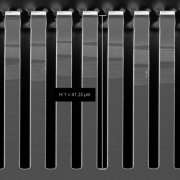
下载SPTS Technologies has been at the forefront of deep silicon etch technology, since the invention of Deep Reactive Ion Etching (DRIE), also known as the “Bosch Process” in 1994. In conjunction with the inventors at Robert Bosch GmbH, SPTS developed the first commercial DRIE system for MEMS manufacturing, and have continued to innovate and improve the processing capabilities throughout the past 25 years. Prior to the invention of this technology the aspect ratio of a dry etched silicon feature was limited to ~10:1 using conventional non-switched techniques.
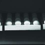
SPTS DRIE technology is used by the majority of leading MEMS manufacturers and foundries to etch deep vertical structures into silicon. In recent years, the applications for deep silicon etching have broadened to include through-silicon via (TSV) etching in advanced 3D packaging, trenches for silicon-based power devices and plasma dicing.
SPTS offers a choice of silicon DRIE modules. For most applications, our latest generation Rapier process module, with its “dual source” design, offers the best performance in terms of CD, profile and tilt control. Our DSi-v module offers higher etch rates and low non-uniformity for non-critical or high load cavity etching, and blanket silicon etching for via reveal or thinning.
To create deep anisotropic etching of silicon, the Bosch Process switches between different plasma chemistries to provide fluorine based etching of the silicon while protecting the sidewall of the growing feature with a fluorocarbon layer. The schematic illustration below shows the 3 main steps of the process which are repeated multiple times to achieve a vertical etch profile. It is a complex but flexible plasma process with key process variables including gas flows, RF power, platen power, and switching times.
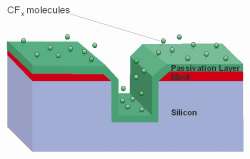
Step 1: A C4F8 plasma deposits a fluoropolymer passivation layer onto the mask and into the etched feature
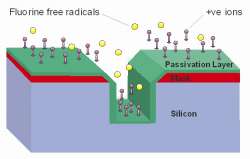
Step 2: A bias from the platen causes directional ion bombardment resulting in removal of the fluoropolymer from the base of the feature and the mask/
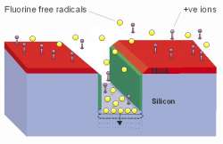
Step 3: The fluorine free radicals, in the SF6 plasma, etch the exposed silicon at the base of the etch feature isotropically, and so the process return to Step 1.
MEMS
| Applications | Typical Requirements |
 High aspect ratio features
|
|
 Microphone and other cavity etches
|
|
Advanced Packaging
| Applications | Typical Requirements |
 Through-silicon via (TSV) etching
|
|
|
Plasma dicing |
|
Power Devices
| Applications | Typical Requirements |
|
Deep trench isolation |
|
End-point control is important for optimizing silicon etch processes, but some features and pattern layouts can be challenging to monitor. SPTS offers a patented* end-point technology called Claritas™. Compared to standard on-chamber OES, Claritas™ provides process control of etches to a stop layer or buried cavities at low open areas (down to 0.05%) or high pressure processes that operate in the 100mT range.
*Patent US 9159599 B2
The link you have selected is located on another server. Neither SPTS Ltd. nor any of its subsidiaries endorses this web site, its sponsor, or any of the information, policies, activities, products, or services offered on the site or by any advertiser on the site. By clicking on the OK button below, you agree and acknowledge the foregoing and will be directed to the selected site.