
XeF2 for MEMS Release
XeF2 vapor etching is a highly selective isotropic etch for removing sacrificial layers of Si, Mo or Ge to release MEMS miccrostructures.
下载In June 2013, SPTS acquired XACTIX, Inc, the leading supplier of XeF2 vapor etch technology, with over 125 etch systems installed at universities, research facilities and device manufacturers. Xenon difluoride (XeF2) can be used to isotropically etch Si, Mo and Ge and is an ideal solution for etching sacrificial layers to “release” moving components within MEMS devices. It provides numerous unique advantages and capabilities compared to wet and SF6 plasma etch options.
As XeF2 is a dry vapor etch there are no surface tension or bubble related problems with etching through small holes or in tight spaces. XeF2 has been used to etch through holes as small as 25nm in diameter. Similarly, XeF2 avoids stiction issues, often associated with wet etch processes which can lead to permanent device damage after release/drying.
As MEMS get more complicated they contain components made from multiple or non standard materials. There is no other isotropic etch that is selective to so many materials. Devices can be made using any combination of silicon dioxide, silicon nitride, polymers, plus most metals and dielectrics.
Because of its selectivity and excellent reach, XeF2 can be used to make very long undercuts with little or no degradation of etch stop, mask or device layers. For example, silicon dioxide is a very popular mask material with a Si:oxide selectivity of >1,000:1. Silicon dioxide masks have been used to achieve very long undercuts (well over 100µm, see Fig 1) and to protect extremely small or thin devices (less than 30nm in dimension).
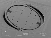
Fig 1 Very long undercuts under a silicon micromirror achieved using XeF2 very thin oxide mask layers (Image Courtesy of Analog Devices, Inc)
The high selectivity of XeF2 to different materials allows a designer to easily incorporate etch stops or to use existing buried structures as etch stops for undercutting. Since there will be almost no attack on the etch stop or the device being released, it is possible to overetch without damage. This means that yield losses due to unreleased and overetched devices can be reduced to zero.
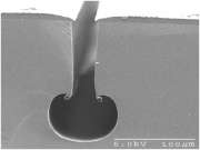
Fig 2 C4F8 passivation layer used to mask sides of DRIE
Low cost photoresist can be used as a cost-effective mask on extended etches, because XeF2 shows minimal attach on polymers. Similarly, XeF2 will not attack the polymer passivation layer which remains on the sidewalls of holes or trenches created using deep reactive ion etching (DRIE). This characteristic can be useful to create tubes or round cavities at the bottom of vertical trenches or holes in a silicon wafer (see Fig 2).
XeF2 does not attack most of the materials typically used in packaging or wafer dicing. As a result, XeF2 can increase yield by delaying the release of a MEMS device until after dicing or package insertion and wire bonding. XeF2 has been used successfully to release MEMS devices on diced wafers on the dicing frame and chips inside packages.
SPTS offers a range of XeF2 etch systems suitable for R&D and production applications
Information on this page contains forward looking information. For more information, click here.

The link you have selected is located on another server. Neither SPTS Ltd. nor any of its subsidiaries endorses this web site, its sponsor, or any of the information, policies, activities, products, or services offered on the site or by any advertiser on the site. By clicking on the OK button below, you agree and acknowledge the foregoing and will be directed to the selected site.