Back-side Metallization for Silicon Power Devices
Introduction
Power devices are semiconductor devices used as a switch or rectifier in power electronics. They are used for a wide range of applications from consumer goods such as washing machines, refrigerators, and cordless drills to electric vehicles (EV), industrial motor control and renewable energy.
In a discrete power device, current flows through the silicon. Electrical contacts are made on both the front and back-side of the die.
To make the back-side connection, after front-side processing is complete, wafers are thinned (to improve electrical performance, or ‘on-state’ resistance), and turned upside down for metal contact layers to be deposited using PVD.
Back-side Metal Process Steps
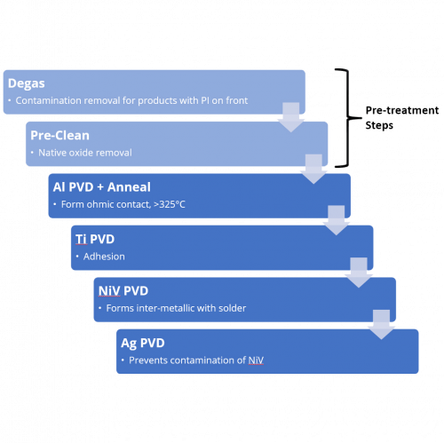
There are several metal layers deposited back-side metallization (BSM), along with pre-treatment steps beforehand to ensure good quality metal is produced with good adhesion, electrical properties and long-term reliability.
 |
 |
| Fig. 1 Individual process steps, common metals used, along with their purpose |
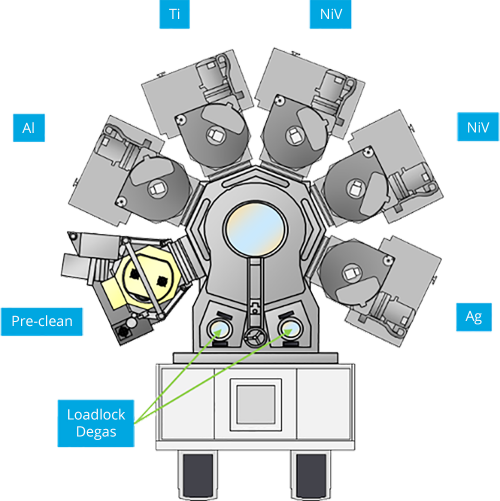
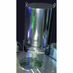
Fig. 2 A typical Sigma® fxP PVD back-side metallization system supporting these steps |
Edge Contact Wafer Handling
With trends towards thinner wafers for improved performance, wafer bow becomes increasingly challenging from a handling perspective. Manufacturers ultimately resort to either using Si strengthening techniques such as the TAIKO thinning process where a full-thickness ridge of Si is left at the edge of the wafer during back-grind, or wafers are bonded directly to carriers.
Consequently, the main hardware requirements for Power BSM PVD processing is to have a handling system that not only supports wafers at the very edge for TAIKO compatibility, but also has capability to handle warped wafers (although TAIKO reduces the problem, it does not totally eliminate it).
Also, because wafers are processed upside down, if carriers or protective tape aren’t used it is important that the ‘active face’ of the wafer is not damaged through direct contact with chamber hardware.
As a result, the Sigma® comes with options for ‘edge contact’ handling, where only the outer edge of the wafer is supported on its journey through the machine. This, together with modified robot velocities allows reliable handling and no front-side damage.
Importance of Degas
With any PVD process it’s important to remove contamination from wafers prior to deposition. Outgassing during deposition can contaminate films, adversely impacting film properties and adhesion. Historically, power devices were fabricated using materials that did not adsorb contaminants, but more recently adoption of organic-based materials such a Polyimide (PI) instead of, or in addition to, PECVD SiN that was traditionally used for passivation.
PI is well-known to absorb moisture when at atmosphere, so removal of this contaminant prior to deposition is important, particularly at 300 mm wafer sizes where the volume of organic material on the wafer is larger.
 |
 |
| Fig.3 Transport Module Lamp Degas Station |
Fig.4 Multi-Wafer Degas (MWD) |
For ultra-thin silicon cases, where the substrate is mounted on rigid carrier such as glass or silicon, bonding adhesives are used which compound the problem, resulting in a need for an even more thorough degas.
For organic passivation cases, a lamp-based degas (shown in Fig.3) in the single wafer loadlocks of the transport module is usually sufficient, but for bonded wafer cases, SPTS's 'multi-wafer degas' (MWD) technology (Fig.4) can offer significant advantages, avoiding throughput bottlenecks caused by the extensive degas time required to fully outgas the wafers at low temperatures. MWD technology is a batch degas design based on IR lamp heating and cryopump vacuum – high vacuum being best practice for contaminant removal efficiency and effectiveness.
Low Damage Pre-Clean
In order to make good electrical contact to the back of the silicon and achieve good adhesion for successful integration and long-term reliability wafers require a pre-clean step after degas to remove and native oxide on the back-side Si that will have formed during exposure to atmosphere. This can be achieving using an offline wet HF dip, or in-situ on the PVD system in a dedicated etch module. In-situ etching has the advantage of eliminating queue time constraints.
Historically, Ar sputter etch technology has been used for the pre-clean step, but to mimimise damage to the Si lattice, lower damage ‘reactive’ etch processes are often used. The Reactive Hot Soft Etch (RHSE) module is an Inductively Coupled Plasma(ICP) source using H2 to chemically remove native oxide, avoiding the high energy ion bombardment of an Ar sputter.
Optimization of BSM Layers
The materials used for the back-side metal stacks vary depending on the device type and the solder used for the subsequent assembly stage but the most common are Ti-NiV-Ag for FETs, and Al-Ti-NiV-Ag for IGBTs.
Conventional PVD modules are used to deposit the layers but with additional features to support thin wafer back-side processing such as 'edge contact' support to avoid damaging the active face, and 'shadow shielding' to prevent metal overspill.
In-situ Al Anneal
For some devices (mainly IGBT), a thin layer of Al or Al alloy is deposited prior to the Ti-NiV-Ag stack. After deposition this is annealed to form a low resistive ohmic contact between the Si and the Al. A temperature of >325°C is required for this reaction to take place. Some remove wafers after Al deposition and anneal them in a dedicated furnace, before returning to a PVD system for the remaining materials in the solder metals stack. To simplify the manufacturing process, the anneal can be performed within the PVD system.
One approach is to cumulatively add heat into the wafer as it continues on its journey around the system after Al deposition, but this has the disadvantage that it relies on consistent, repeatable wafer scheduling and chamber pump recovery performance between wafers, to ensure optimal wafer to wafer repeatability. It also limits stress control options for subsequent metals where temperature reduction is usually employed.
Another approach is to send the wafer to an anneal station, or even back to a loadlock for a lamp-based anneal, which has negative implications for throughput.
The Sigma® fxP performs the Al anneal function in-situ, and in the Al deposition chamber itself, avoiding any of the scheduling or vacuum recovery concerns from the alternative approaches.
Evidence of successful ohmic contact can be observed by removing the Al layer post-deposition using a wet etchant and inspecting the surface of the silicon. Regular pyramidal divets in the Si indicates successful inter-diffusion between the Al and the Si, forming the desired low-resistive contact.
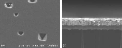 |
Fig. 5 (a) Pyramidal features indicative of Si junction spiking
(b) Cross-section of Al-Ti-NiV-Ag stack showing Al-Si inter-diffusion |
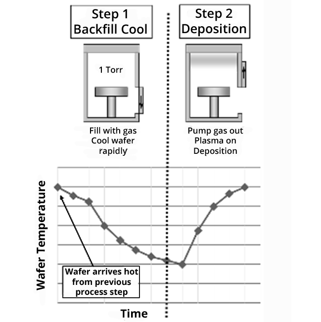
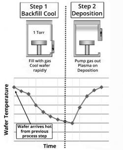
Stress Control
Following deposition of the Al layer, deposition of the remaining layers is performed as cold as possible, to minimize extrinsic stress and subsequent warpage. We use a 'backfill cool' technique to remove heat from the wafers, either as they arrive from a previous hot process, or during the deposition. The 'backfill cool' technique is non-clamped approach to heat transfer, that involves increasing chamber pressure to a level that will conduct heat away from the wafer to a chilled platen beneath, before opening up vacuum valves and initiating the sputter deposition process.
 |
 |
| Fig. 6 Backfill Cool Technique to remove heat from thin wafers |
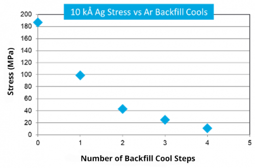
Fig. 7 Impact of backfill cool steps on 10kA Ag film stress |
In addition to the 'backfill cool' technique, pulsed DC, N2 addition and traditional pressure adjustment can be used. Having multiple stress control parameters allows the Sigma® to tune wafer bow. In some cases, wafers with larger incoming bow can be delivered from the PVD machine effectively flat – ideal for processing further down the line.
In the case of thin Si mounted on carriers, wafers will be flat, and more robust, so the use of 'cold electrostatic chuck' (ESC) technology is an option to remove heat from the wafers more efficiently, increasing throughput.
Summary
Depositing back-side metal for power devices has multiple challenges, particularly on 300 mm: handling thin, warped wafers without damaging the front-side, removing contaminants from organics without impacting throughput, removing native oxide without damaging the silicon, annealing aluminum to form an ohmic contact, and depositing metal layers with low stress to minimize wafer bow.
The Sigma® fxP has been designed to meet all of these requirements, using edge contact processing, batch vacuum degas, low damage etch, and backfill processing to either put heat into wafers for ohmic contact or take heat out for stress control/bow reduction – a relatively efficient approach to heat transfer that is compatible with fragile, thin wafers and proven in production.