
PVD Metallization for SiC Power Devices
Introduction
Applications such as electric vehicles, rail transport and industrial motors are driving the demand for new power devices capable of switching higher power and voltages, often in harsh environments, with a small form factor and high reliability.
Silicon carbide (SiC) is one of the primary wide bandgap (WBG) semiconductor materials used to address these challenging requirements. SiC will operate at much higher temperatures and withstand up to 10 times stronger electric fields while having the same dimensions as a silicon (Si) power device. According to Yole[1] the SiC power device markets will reach $2.5B by 2025.
Currently volume production of WBG power devices at 100mm and 150mm wafers is “the norm”, but several power device manufacturers are now progressing to realize the cost benefits of scaling to 200mm wafer formats.
The SPTS Sigma® fxP physical vapor deposition (PVD) system is well-established in Si power management fabs on wafer sizes up to 300mm, and can also be used to process ≤200mm SiC wafers for both frontside and backside metallization.
Metal Deposition for SiC Power Devices and Key Challenges
Engineers depositing metal films onto SiC experience similar PVD challenges as those faced when depositing onto Si, namely producing low defect metal with strong adhesion, good electrical properties and long-term reliability, while maximizing tool productivity. Just like Si devices, in SiC, there are two main applications; frontside thick metal conductors and backside solderable metal stacks.
The wafer frontside is processed with thick Al alloy conductors. These are quite thick in the range of 3-5µm to handle high currents. Ti – TiN diffusion barriers can be used as in Si processing, and can aid the Al processing that follows. The ohmic contact is formed with Ni, not Al as is normal in Si power devices, because Al would evaporate at the high temperatures needed to form a silicide with SiC. Challenges of frontside processing include avoiding defects in the thick Al while maintaining productivity and depositing the materials into increasingly higher aspect ratio features.
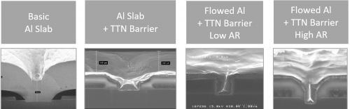
Fig 1 SEMs illustrating increasing complexity/aspect ratio of frontside features found in typical discrete Si and SiC power devices
To make the backside drain contact, as with Si power devices, the SiC wafers are thinned to reduce “on” resistance. When processing the backside, contact on the active face side of the wafer must be avoided to prevent device damage. A PVD solderable metal stack is then deposited consisting of Ti for adhesion, Ni or NiV for the intermetallic, and a final layer of Au or Ag to protect the intermetallic layer when in storage prior to final assembly.
Total stress management of the PVD stack is critical. Any stress of the metal stack can lead to adhesion issues, and potential handling issues if the wafer bow exceeds the limits of the wafer handling capability.
Benefits of using Sigma® fxP PVD for SiC Power Devices
|
Productive degassing and pre-clean prior to deposition steps |
Using a heated platen and high pressure Ar, SPTS’s Soft Etch module can both degas and pre-clean wafers, although throughput can be increased if a dedicated heat module is added to the Sigma’s configuration. The Soft Etch module generates a high ion flux and controlled ion energy, to provide high rate, low damage pre-clean processes. Metal shielding allows etching of metals and polymers on the wafer and ensures high MTBC typically >10-15k wafers. |
|
Flexible and extendible options for Ti/TiN barrier deposition |
Choice of Standard, Hi-Fill® (HF) and Advanced Hi-Fill® (AHF) modules for increasingly higher aspect ratio features. A Standard PVD module can be used to deposit barriers with aspect ratio up to 1:1, and can be upgraded to HF or AHF by changing the top half of the module, without the cost of replacing the whole module. The ionized PVD AHF module provides good step coverage of high density diffusion barriers into high aspect ratio (>2.5:1) vias. |
|
‘Best In Class’ productivity for thick Al films |
High throughput thick Al alloy films with greater than two times the wph of competitive systems. Fewer, faster PMs, means highest productivity and lower CoO. |
|
Avoid defects/whiskers during deposition of thick frontside metal without loss of productivity |
Clampless processing means fewer defects, no sticking wafers, and no need for expensive electrostatic chucks. Low contamination levels within the chamber means the growing film stays clean and virtually defect-free. The Sigma® fxP system will deposit thick Al alloys at rates >1.3µm/min, without the whiskers common on other PVD systems. |
|
Reliable wafer handling |
Thinned SiC wafers are expensive. Using the same techniques developed for Si BSM deposition, we specify wafer breakages of <1 wafer per 100k. The Sigma® fxP also has options available to allow reliable sensing and tracking of transparent SiC wafers, as well as standard Si wafers used for chamber conditioning. |
|
Frontside protection during back side metallization |
Wafers are handled through the system by contacting only the very edge of the wafer, meaning the active frontside is completely protected from scratches and defects. Shadow shielding stops backside metal transferring to the device side for maximum yield |
|
Stress control to prevent wafer bow and improve adhesion |
The Sigma® fxP manages film stress via multiple stress control options. Our unique and efficient Backfill Cool feature uses wafer temperature to control stress. Combined with pulsed DC, and NiV+N2 options, our Sigma® delivers optimal controllable stress with very competitive throughputs, leading to ‘best in class’ device yield. |
Summary
SPTS Sigma® fxP PVD system offers many unique features that have proved critical to high volume manufacturing of both Si and SiC power devices, in terms of maximizing the device performance, yields and wafer throughputs. For further details, contact your local SPTS Sales Team or email enquiries@spts.com
References
[1] “Power SiC: Materials, Devices and Applications 2020”, Yole Développement (Nov 2020)