
Etch Processes for WBG Power Devices
This Application Brief describes SPTS etch processes for SiC and GaN-on-Si power devices, using our ICP and Synapse etch modules
다운로드Power semiconductor devices, such as diodes, switches and amplifiers, constitute the heart of power electronics systems, controlling the flow of electricity. Historically silicon-based power devices have been the dominant choice, due to their low cost and good electrical performance. However, emerging applications such electric vehicles, high speed rail and fast charging are depending more heavily on the wide bandgap materials (SiC and GaN) due to their higher operating voltages and faster switching capabilities. SiC has become the material of choice for high power/voltage devices exceeding 650V. While SiC devices only account for about 4% of the total power device market in 2020, analysts forecast a CAGR of >30% over the next 5-7 years when the market will reach $1.5B. GaN-on-Si devices, on the other hand, compete with Si devices in the range 600-650V but represent a much smaller market (<1% of total power devices). These devices are also expected to grow significantly over the next 5 years.
Etching SiC is a particularly challenging process since the material has a hardness approaching that of diamond. It also has a very stable chemical structure. This makes it more difficult to dry etch than other compound layers such as GaAs, AlGaAs or InP, which have more chemical etch mechanisms requiring conventional inductively coupled plasma (ICP) process modules. For SiC SPTS offers its unique Synapse™ process module. Originally designed for deep etching of oxide it is also well suited to SiC because of the more physical plasma environment. Synapse etch rates for oxide and SiC are typically 2-3 times faster than in a standard ICP.
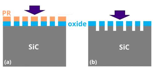
Fig 1 Schematic showing (a) hard mask open and (b) front-side SiC trench etch
Oxide Mask Open
Silicon oxide is used as a hard mask which can withstand the aggressive etch conditions required to etch SiC. Key requirements for the mask open step are high oxide etch rate for productivity, with a vertical profile for accurate profile control of the subsequent SiC trench etch, and minimal loss of the under-lying SiC. This requires accurate end-point detection using OES (optical emission spectroscopy) and control of the etch uniformity across the wafer.
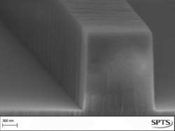
Fig 2 Oxide mask etched at 0.45µm/min with 15nm of SiC loss and uniformity<±1%
Shallow (front-side) SiC trench Etch
Power devices often use vertical trench-shaped structures to reduce the on-resistance and increase the packing density compared with traditional planar designs. These trenches are typically 1-2µm deep with widths from 0.5-1.5µm. The trench base requires no micro-trenching to ensure the gate oxide quality, void free filling with polysilicon and to prevent high, localised electric fields leading to breakdown. For next-generation devices operating at yet higher voltages, manufacturers are looking to completely avoid any form of corner in the trench by forming a trench with a rounded base. This is a difficult profile to achieve in wider/shallow SiC trenches, but by careful control of the etch/passivation chemistry, polymer build-up on the sidewalls can reduce the etching at the base corners of the trench creating a rounded shape. The polymer passivation can easily be removed by a post etch wet clean. The approach gets easier as the trench CD reduces and the aspect ratio increases. Examples of SiC trench etches are shown in Fig. 3.
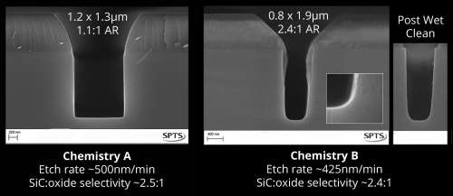
Fig 3 Two examples of shallow front-side SiC trench etches
To ensure wafer-to-wafer repeatability in production, this shallow trench process can be end-pointed by white light interferometry but only if the etching area is high enough. LASER interferometry can be used for any trench open area but requires the 25µm diameter spot to be placed inside a target feature of ~350µm (reducing to ~250µm when pattern recognition software is selected). A correlation can then be made between the depth of the target feature and the depth of the real trenches to ensure accurate wafer to wafer trench depth control.
Front-side Etch Processes
There are a number of different front-side etch processes which may be needed for GaN-on-Si power devices, depending on the process route and final desired structure. Generally, these are shallow etches of SiNx or of epitaxial GaN or AlGaN. These require controllable low etch rates, low operating powers to minimise plasma induced damage and high selectivity to under-layers to minimise the loss of thin layers. Automated end-point detection is essential for process control.
SPTS’s ICP module is well suited to these etches and can be operated at low source power (down to 50W) and low bias power (down to 6W) by operating the RF generator in HALO (High Accuracy Low Output) mode. There is also an option to pulse the bias power leading to a net power <6W. Attenuation of the bias power may also be used (to 3W) but this leads to poorer accuracy of the power level compared to HALO mode.
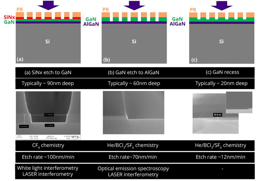
Fig 4 Schematic illustration of three critical frontside etch steps for GaN-on-Si power devices with recommended plasma chemistries and end-point detection options.
Back-side Through Silicon Via (TSV)
Finally, there may be a requirement to etch a TSV interconnect from the back of the wafer to the underside of the frontside metallization. SPTS Technologies has been at the forefront of silicon DRIE technologies for over 25 years. Our Omega® Rapier offers high etch rates for productivity, smooth sidewalls for ease of TSV passivation/metallization, and patented Claritas™ end-point detection which can monitor the progress of the via etch even when the TSV density is as low as 0.05%.
To find out more about SPTS’s etching capability for WBG materials in power device applications, you can listen to a recording of a technical webinar from April 2020 , or Contact Us for further details.
Information on this page contains forward looking information. For more information, click here
The link you have selected is located on another server. Neither SPTS Ltd. nor any of its subsidiaries endorses this web site, its sponsor, or any of the information, policies, activities, products, or services offered on the site or by any advertiser on the site. By clicking on the OK button below, you agree and acknowledge the foregoing and will be directed to the selected site.