
AlN-AlScN Etch for BAW Devices
In this Application Brief we give an overview of the benefits of the Synapse module for etching AlN and AlScN for BAW device manufacturing, in terms of high etch rate, sidewall angle and end-point control
다운로드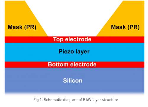
Piezoelectric thin films are commonly used as the resonator in bulk acoustic wave (BAW) devices for RF filtering in mobile phone handsets. AlN is the base piezoelectric material but recent trends involve doping heavily with scandium (Sc) to improve the coupling efficiency, which allows thinner resonators for higher frequency operation, as we move towards 5G communications. Device makers are currently working with Sc content typically in the range 6-30at%.
Fig 1 illustrates a typical structure which needs to be etched to create a BAW device, with the piezoelectric layer sandwiched between the two metal electrodes. There are a number of steps in the process (1) etching through the top electrode, then (2) etching the piezoelectric layer, stopping on the bottom electrode with minimal bottom electrode loss and (3) etching the bottom electrode. As with all production processes, WIW and WTW non-uniformities should be controlled to maximise device yields.
As feature sizes have reduced over time, the industry has also moved from wet etching to dry etching to define the piezoelectric layer and the associated metal electrodes. Unfortunately, increasing the Sc content makes dry etching more problematic because of the low volatility of scandium halides relative to those of Al and N.
High Etch Rate
For production applications, device manufacturers require a high etch rate to improve productivity. As scandium content increases in the AlN it becomes harder to etch. Standard ICP reactors are capable of etching un-doped AlN and AlScN with up to ~10at.% Sc AlN at ~600nm/min. However, to future-proof your processing capability, SPTS recommends their Synapse™ etch system which has a unique source design offering a higher ion density, engineered specifically to etch strongly bonded materials, also including oxides and SiC. Recent work has found that at low scandium content the etch rate of the SPTS Synapse™ is comparable to an ICP. Every reactor will see a fall in the etch rate as Sc levels increase but the reduction in the case of an ICP is far greater than for the Synapse. The effect is so significant that the ICP approach above 25at% Sc is no longer viable compared to the Synapse that can still deliver ~260nm/min and at 30at.% Sc 100nm/min is still maintained (see Fig 2).
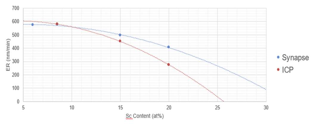
Fig 2 Effect of Sc content on etch rate in standard ICP and Synapse modules
As the process etches through the bulk of the AlScN layer and nears the bottom electrode, the process parameters are typically changed so as to land softly on the electrode and minimise the loss. Soft landing steps are typically slower than main etch conditions and so the etch rate arguments above are exacerbated. Typical soft landing conditions can deliver lower electrode loss in the 10-20nm range.
Sidewall angle
For BAW devices a typical sidewall angle of the piezo layer etch would be between 10 and 45o. Tapering like this is generally preferred for subsequent coverage by thin films. This is achievable using a Cl2 based plasma in a SPTS Synapse™ module and by paying attention to the incoming mask profile. As device geometries reduce customers are looking for steeper sidewalls so that the features occupy less real-estate. In cases where AlScN is used for MEMS devices the profile in the piezoelectric layers are typically required to be steepest at >70°. A common problem when etching any low volatility film such as AlScN is re-deposition of by-products on to the wall or the mask of the etching feature as these can be difficult to subsequently remove and can also impede the etch front. The more physical nature of the SPTS Synapse process and the lower operating pressure available means that re-deposition can be more easily managed than in an ICP. This allows the SPTS Synapse to produce more vertical profiles with less re-deposition.
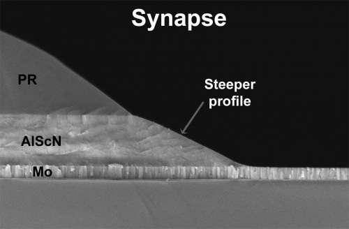
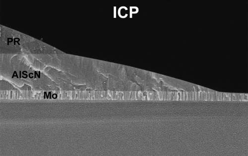
Fig 3 Comparison of profile of AlSc15at%N in Synapse™ and standard ICP
Electrode Etch
The top Mo electrode is typically 200nm thick. It is possible to etch Mo in either an ICP or SPTS Synapse™ module using a Cl2/SF6 plasma chemistry. When more ‘inert’ electrodes are preferred, like Pt or Ru, the SPTS Synapse™ becomes the better choice. It is possible to tune the Mo profile by altering the PR selectivity of the process. For example Mo profiles in the range 10-54° are obtained by process adjustment when the incoming PR mask is ~40°.
End-point Control
End-point detection is essential to stop the etch at the required point, when etching the Mo top electrode to the piezo-electric layer, and the piezo-electric film to the bottom electrode. In both of these process steps Optical Emission Spectroscopy can be employed which monitors one of the light emitting species of the plasma. End-point detection control improves wafer-to-wafer repeatability and can help to manage any variations in layer thickness or etching rate.
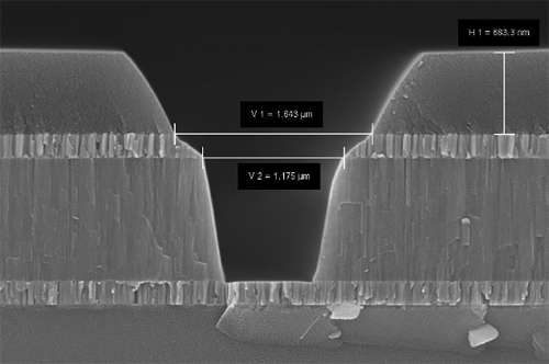
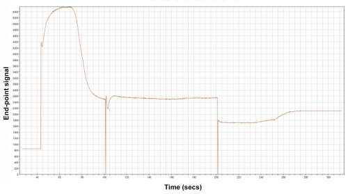
Fig 4 Profile of Mo/AlN/Mo Stack etch, with associated OES end-point trace
The SPTS Synapse™ etch system offers significant advantages over ICP approaches when etching for BAW manufacturing, in terms of productivity, selectivity and profile control for AlN/AlScN piezo-electrics and for electrode materials. The physical nature of the process is increasingly beneficial as the scandium content increases over time. This future-proofs the approach with respect to the emerging 5G applications where an ICP is no longer viable.
The link you have selected is located on another server. Neither SPTS Ltd. nor any of its subsidiaries endorses this web site, its sponsor, or any of the information, policies, activities, products, or services offered on the site or by any advertiser on the site. By clicking on the OK button below, you agree and acknowledge the foregoing and will be directed to the selected site.