
Plasma Etch End-point Control
End-point detection (EPD) is essential for many wafer etch applications to ensure processes are carefully controlled and consistent.
다운로드End-point detection (EPD) is essential for many wafer etch applications to ensure processes are carefully controlled and consistent, to ensure reliable results are achieved wafer-after-wafer, and optimize device yields.
There are many methods used to end-point wafer processes and this webpage aims to describe the techniques available for SPTS’s range of etch modules. The techniques either monitor the wafer thickness, analyze changes in the chemical/optical properties of the plasma above the wafer, or monitor the system datalogs.
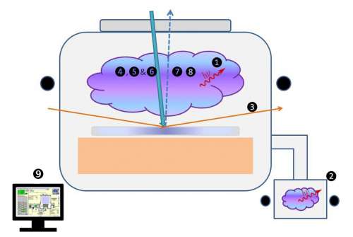
Fig. 1 Illustration showing various SPTS EPD options
|
|
|
|
ICP |
Synapse |
DSi & DSi-v |
Rapier |
Notes |
|
(1) |
OES (Ocean, Spectraview, Filter Diode) |
Most etches to a stop layer, multi layer stacks (e.g. VCSELs), inter-wafer cleans for DRIE |
✔ |
✔ |
✔ |
✔ |
|
|
(2) |
Claritas™ |
DRIE etches to a stop layer or buried cavity.Inter-wafer cleans for DRIE |
|
|
✔ |
✔ |
Requires OES in combination <0.05% open area capability |
|
(3) |
ReVia® |
Via Reveal |
|
|
|
✔ |
|
|
(4) |
NIR |
Si thinning |
|
|
✔ |
✔ |
For final Si thickness ≤45μm |
|
(5) |
White Light Reflectometry |
Tapered Si vias. Multi-layer stacks (e.g. VCSEL) |
✔ |
✔ |
✔ |
✔ |
Common hardware |
|
(6) |
White Light Interferometry |
Shallow, blind etches (e.g. Si or glass) |
✔ |
✔ |
|
|
|
|
(7) |
Laser Interferometry |
Compound epi or SiC trench etch |
✔ |
✔ |
|
|
|
| (8) | Ascent™ | SiC via etch processes with metal masks | ✔ | Insensitive to open area or via diameter | |||
|
(9) |
Parameter |
Etch where end point is accompanied by a change in datalogged parameters |
✔ |
✔ |
✔ |
✔ |
(1) Optical Emission Spectroscopy
Optical emission spectroscopy (OES) is a technique used to analyze the light spectra emitted by a plasma during an etch process. The main advantage of OES is that it is a whole wafer technique, requiring no alignment of individual wafers, and tends to be lower cost than interferometry options. However, this method requires a stop layer, or differing layers. When the exposed area is small or the different layers are similar in composition then the change in the emission intensity is also small and can be difficult to detect.
(2) Claritas™
Claritas™, a patent protected technology (Patent US 9159599 B2) from SPTS, extends the use of existing OES options available on SPTS etch modules and enhances the detection of reactants and/or by-products. It allows end-pointing for applications even with low exposed areas (down to 0.05%) or “high pressure” processes that operate in the 100mTorr range. Claritas™ can be used for most Si etches to a stop layer as used for MEMS and TSVs (vertical via-last).
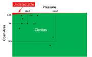
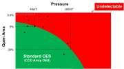
Fig. 2 Graphs illustrating enhanced capability of Claritas™ for low exposed area and/or high pressure processes
(3) ReVia®
ReVia® is a unique (Patent US 8709268 B2) end-point technique for in-situ monitoring the “via reveal” etch process. It detects the emergence of the vias during the backside etching of thinned wafers, in “via-middle” 3D-TSV packaging applications. It is capable of successful end-pointing even at remarkably low (<0.01%) via densities, and can save time and minimize yield loss in volume manufacturing.
(4) Near Intra-Red (NIR)
The NIR technique uses the transparent nature of silicon to infra-red to monitor the change in wafer thickness during a silicon thinning process. With reflections off buried layers, or the opposite face of a silicon wafer, this approach can be used to end-point the thinning etch at a target thickness within 45μm of the reference surface.
(5) White Light Reflectometry
Reflectometry (and interferometry) relies on an external light source which is directed onto the wafer. The reflected light is detected and analyzed. If there is a stop layer with a different reflectivity then there will be a clear end-point signal produced. Reflectometry can be used for tapered TSV via-last etches.
(6) White Light Interferometry
Incident light will transmit through the wafer i.e. no window in the mask is required and be reflected from the interfaces between the layers, and the bottom of the etch feature, as well as from the top surface.
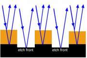
Fig 3 Schematic diagram of white light interferometry
These reflected beams will interfere with each other, either constructively or destructively, creating a sinusoidal intensity signal with periodic oscillations called “fringes”. The number of fringes will change with the changing depth of the etch front and mask thickness as it etches away (while the mask-wafer interface remains fixed), thus enabling real-time depth control and a measure of mask selectivity.
(7) Laser Inteferometry
A window is required in the mask at the wafer centre to take the LASER spot which is 15-20µm diameter. The window is 300-1200µm wide for the standard set-up but when optional pattern recognition is taken this reduces to 100-400µm. The smaller window sizes correlate with the better wafer placement accuracy of the automated c2L and fxP handlers, compared to the manual LPX. Two LASER wavelengths are available - 670nm is typically used for VCSEL stacks on GaAs wafers or SiC trench etch and 980nm is typically used for InP.
(8) Ascent™
Ascent™ is a unique (patent applied for) solution for in-situ endpoint of deep backside SiC vias to GaN for high power GaN-on-SiC RF devices. It is compatible with metal masks which prevent the use of OES. It can end-point layouts with small via diameters and low open areas, with autofocus to allow for substrate thickness variations. No costly pattern recognition is required.
(9) Parameter
System datalogs monitor many parameters of the etch process & process module including pressure, platen temperatures, RF matching, Vpp etc. In some cases, these parameters will react in the event of some change on the wafer, e.g. etch front reaching a cavity, allowing helium backpressure flow to escape or changing stress on wafer. The datalog can be used to monitor for these changes as the etch progresses triggering end-point as required.
For more details about the benefits of an appropriate end-point solution for your process / SPTS system, contact your local sales team
Information on this page contains forward looking information. For more information, click here.
The link you have selected is located on another server. Neither SPTS Ltd. nor any of its subsidiaries endorses this web site, its sponsor, or any of the information, policies, activities, products, or services offered on the site or by any advertiser on the site. By clicking on the OK button below, you agree and acknowledge the foregoing and will be directed to the selected site.