
SiC Etch for Power & RF Devices
Introduction
Etching SiC is a particularly challenging process since the material has a hardness approaching that of diamond. It also has a very stable chemical structure. SiC is more difficult to dry etch than some other compound layers e.g. GaAs, AlGaAs, InP, which can be etched in a conventional inductively coupled plasma (ICP) system.
The etch rate of SiC in a conventional ICP system is typically only <0.5µm/min, which is too slow for deep backside via etching. Over a decade ago, SPTS developed an enhanced ICP source which creates a more energetic plasma with a higher ion density which offers significantly (2-4x) better etch capability for SiC and other “hard-to-etch” materials like silicon oxide. The latest generation of this enhanced plasma source is the Synapse™ etch module.
Dry etching SiC vias is a very “dirty” process with each wafer sputtering ~30mm3 of Ni (from the mask) & releasing 15mm3 of C & Si. To combat this issue, the Synapse™ module incorporates heated walls to minimise by-product build-up and increase MTBC, and specially designed chamber shielding to reduce MTTC.
GaN-on-SiC RF Devices
GaN is a wide bandgap material which is commonly used in high power and high frequency RF applications. Due to the difficulty and high cost of producing defect-free bulk GaN wafers, GaN is usually deposited as an epitaxial layer onto SiC (or silicon) substrates. To create an interconnect from the backside of the substrate to the active frontside GaN, it is necessary to etch a deep via through the SiC. This process is carried out on thinned wafers mounted on a carrier of SiC or sapphire.
For backside SiC via etching the etch rate is important to ensure a high throughput, and the sidewall smoothness and angle must be suitable for subsequent metal lining/plating. The high ion energy to achieve high etch rates tends to induce microtrenching near the sidewall, so a good selectivity to the GaN layer underneath is essential to allow sufficient overetching to clear all the SiC from the bottom of the via, without etching the GaN layer too much. Deep etches are possible with a mechanically assisted ESC to maintain consistent wafer temperature and the bonding integrity with any carrier wafer (See Fig. 1).
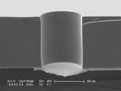
Fig. 1 Backside via etch, 80µm deep @1.9µm/min
(Courtesy of ETRI [1])
A second etch process is then required to etch through the GaN base layer. With the Synapse™ both SiC and GaN can be etched in the same process module (See Fig. 2)
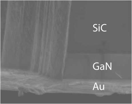
Fig. 2 GaN etch to underlying Au layer
SiC Power Devices
Power semiconductor devices, such as diodes, switches and amplifiers, constitute the heart of power electronics systems, controlling the flow of electricity. Silicon-based power devices have been the dominant choice for this system, due to their low cost and good electrical performance. However, as the needs for electrical energy and higher power continuously grow, for example from emerging applications like renewable energy conversion and electric vehicles, SiC has become the material of choice for next generation high power/voltage (>900V) applications. IHS forecasts[2] that the market for SiC power devices will expand to just over US$3 billion by 2025, driven primarily by hybrid/electric vehicles (see Fig. 3 below).
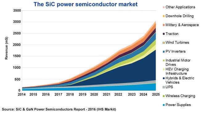
Fig. 3 SiC power semiconductor market forecast (Source: IHS)
The wider bandgap, higher thermal conductivity, and larger critical electric field allow SiC devices to operate with faster switching times at higher temperatures, higher current density, and higher voltages with lower power losses than silicon power devices. These enhanced material/electrical properties of SiC however must outweigh the many disadvantages when compared to silicon, which include much higher wafer costs, limited wafer size (only up to 6”, so fewer devices per wafer) and the challenges in etch processing previously mentioned.
Power devices often use vertical trench-shaped structures to reduce on-resistance compared with traditional planar designs. These trenches are not as deep as backside via structures in RF applications, but micro-trenching at the bottom edge of the power trench is a common issue which can result in a cavity after lining/filling, or increase the peak electric field and induce the breakdown of the device. The etch process must be carefully optimized/controlled to avoid trenching, as shown in Fig. 4.
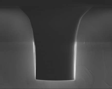
Fig. 4 Power trench with no micro-trenching
If required, high aspect ratio trenches can be achieved. Recent published results[3] have quoted aspect ratios ~25:1.
Download the Application Brief
To find out more about SPTS’s SiC etching capability, contact your local sales team, or Contact Us.
References:
[1] “Backside Via Process with Defect Free Sidewalls for GaN MMIC Applications”, Kyu Jun Cho etc al Proc. CS Mantech 2017
[2] “SiC and GaN Power Semiconductors Device Report 2016” IHS Markit
[3] “High Aspect Ratio Vias in Silicon Carbide Etched by Inductively-Coupled Plasma”, M Tadjer et al, Proc. CS Mantech 2017
Information on this page contains forward looking information. For more information, click here