
Advanced Packaging Webinar Series Part I - Low Temperature Dielectric Deposition for Advanced Packaging
Advanced packaging continues to proliferate within semiconductor device manufacturing, offering performance benefits beyond those of front end of line (FEOL) CMOS gate length scaling only. Through silicon vias (TSV) and hybrid bonding both enable a shortening of the interconnect path with the lower resistance giving reduced parasitic losses and consequent higher device operating speeds and lower power consumption. These advanced technologies allow the stacking of die into 3D packages and so increase device functionality without any increase of package footprint; a particular benefit for mobile devices where low power consumption and small footprint are absolute requirements. An ever-increasing number of applications are realizing the benefits of such solutions, including stacked CPU and SRAM for logic and stacked DRAM for high bandwidth memory (HBM).
 Dielectric materials are key building blocks in advanced packaging schemes, serving a number of quite different, but equally important, roles such as electrical isolation, passivation, bow compensation, bonding interface and inter-die gap-fill.
While spin-on dielectrics (SoD) are attractive because of their relatively low processing costs there are significant disadvantages to their use in an increasing number of packaging schemes relating to thermal budget, stress control, thickness control and compatibility with downstream process integration flows. Low temperature PECVD dielectric layers are increasingly preferred.
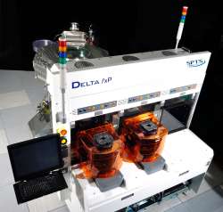
In this webinar we will demonstrate how high quality PECVD dielectric films can be deposited at temperatures as low as 100°C while maintaining high film quality and stability. We will then discuss the use of these films in a number of advanced packaging applications.
Registration is required for this online event :
Date: Wednesday 25th August 2021
Session 1: 08:00am UK (BST) / 09:00am Europe / 15:00pm China & Taiwan / 16:00pm Korea
Repeat Session: 09:00am PDT / 12:00pm EDT / 17:00pm UK / 18:00pm Europe
N.B. The same content will be shared in both live broadcasts, listed above, to accommodate all time zones.
Presenter: Keith Buchanan, Senior Product Manager, PECVD

Keith Buchanan is the Senior Product Manager, PECVD at SPTS Technologies. He graduated from the University of Glasgow with B.Sc. Electronics & Electrical Engineering in 1984.
He has over 25 years of experience in the semiconductor industry, joining Electrotech in 1998. Through a series of acquisitions and mergers, Electrotech became Trikon, Aviza Technology, and finally SPTS in 2009. Keith has previous experience in process development and wafer fab process integration for MEMS and photovoltaic applications and has been responsible for product marketing of SPTS PECVD technology within Packaging, MEMS, and other end markets for the past 8 years.