
Plasma Processes for VCSELs
New applications for VCSELs include proximity sensing for automotives and gesture/face recognition for consumer products and SPTS offers a range of processes for VCSEL manufacturing including ICP etch, PVD, and PECVD.
下載While Vertical Cavity Surface Emitting Lasers (VCSELs) have been used in data communications for over 20 years, there are a host of emerging applications that are boosting demand for VCSEL production and performance. These include applications such as proximity sensing, infrared illumination/heating, atomic clocks, high-resolution video display, and gesture/facial recognition. Market researchers[1-3] forecast the global VCSEL market will grow at a CAGR of between 17-23% over the next 5 years.
Generally, the advantages of VCSELs over alternatives like Edge Emitting Lasers (EELs) and Light Emitting Diodes (LEDs) are low cost and optical efficiency, within a small footprint. They further have the advantage of wavelength stability over temperature and are directionally focused to maximize output efficiency. As VCSELs are top emitting (as are LEDs), they may be integrated with simpler optics and can be mounted as dies on printed circuit boards or integrated with a laser, driver, and control logic all within the same package. Power output is easily scalable by creating arrays of individual VCSELs.
Example: VCSELs for LiDAR for automotive applicationsOne application, that is currently driving much research and product development, is the use of VCSELs in Light Detection And Ranging (LiDAR), which is a technique for monitoring relative distances and movement, essential for the development of autonomous vehicles. LiDAR works in a similar way to radar, but emits pulsed light instead of radio waves to reflect off surrounding objects. The “time of flight” for the reflected pulse to return to the LiDAR sensor is used to calculate the relative distance from the object. The shorter wavelength of the UV/visible/IR light (10-3µm-100µm), compared to the wavelength of radio waves (~1mm) enables detection of smaller objects and higher definition images. The most common VCSEL epitaxy combination is GaAs/AlGaAs, which emits light in the red/near-infrared spectrum (wavelength~700-1100nm). To obtain longer wavelengths, VCSEL manufacturers need to move to other materials like InP or GaN, which are much harder to produce due to various factors, and consequently more expensive. |
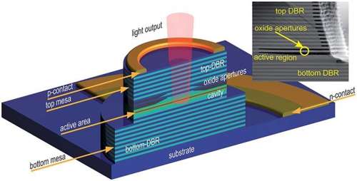
Fig 1 Schematic diagram of a typical GaAs-based VCSEL[4]
A VCSEL is created from a complex multilayer structure (See Fig 1) that is deposited onto the substrate by Molecular Beam Epitaxy (MBE) or Metal Organic Chemical Vapor Deposition (MOCVD). The epitaxial layers will include an active layer that produces the photons, sandwiched between two distributed Bragg reflectors (DBRs) that act as mirrors to reflect the light back and forth through the active area multiple times to enhance amplification. Each DBR is made up of many epilayers in “mirror pairs” (typically >20 pairs), with the refractive index and thickness of each epilayer being tailored to induce constructive interference of the light of the desired wavelength.
An “aperture” can be created to confine the current into a small area of the active layer by selective ion implantation or oxidizing certain epitaxial layers (e.g AlGaAs layers in the case of GaAs-based VCSELs are partly oxidized creating a non-conductive region around the aperture). This concentration of current flow lowers the threshold current to produce laser emission and controls the beam width.
In line with market forecasts, SPTS has seen VCSEL activity ramp significantly for consumer and automotive applications since 2H 2016. Manufacturers are selecting our etch, PECVD, and PVD solutions because of our extensive process libraries and years of experience in related technologies such as GaAs RF and LED manufacturing.
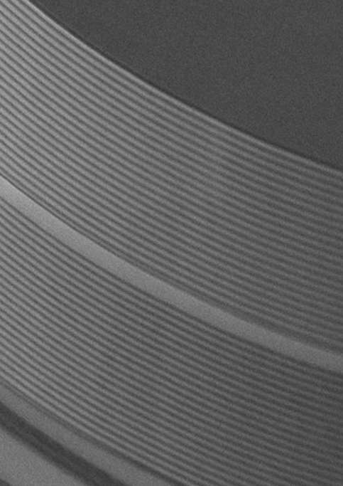
Fig 2 Tapered VCSEL etch with smooth sidewall surface
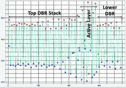
Fig 3 Laser Interferometry data for end-point control in VCSEL etching
Inductively coupled plasma (ICP) is used to etch the mesa structure of the VCSELs. SPTS’s Omega® etch systems are producing vertical and tapered profiles in volume production. The key requirement for next generation VCSELs is for a smooth etch, with no sidewall damage or preferential etch of any of the layers. An uneven sidewall could lead to optical losses from the side of the VCSEL. This profile is very difficult to achieve using wet etching, that is isotropic in nature, and could lead to notching into the epi layers. SPTS also offers a choice of end-point options using fringe counting by laser interferometry or OES for optimum process control in production.
SPTS’s Sigma® PVD technology is used to deposit TiW/Au seed layers (using our Hi-Fill module), and Au for contacts that supply the current or aid heat dissipation from the frontside of the device. PVD layers with tailored stress properties can also be deposited to compensate for wafer stresses, which would otherwise cause warpage once a wafer is thinned and debonded from a carrier.
SPTS’s Delta® PECVD systems are used by VCSEL manufacturers to deposit silicon nitride layers of the highest quality. The most critical application is the surface anti-reflective coating which improves laser performance. Here, the lowest possible non-uniformity of thickness and refractive index is required and SPTS offers industry leading film performance on a high productivity platform. Silicon nitride is also used to provide sacrificial stress compensation layers that minimise the bow and warpage of thinned substrates, and also passivation and hard mask layers.
Related Links
In March 2017, SPTS partnered with the Compound Semiconductor Centre, Swansea University and Cardiff University on a 12-month UK Government-funded project to improve/develop various processes, including ICP mesa etching from SPTS, for high volume production of GaAs/AlGaAs VCSELs on 150mm substrates[5].
Established in July 2017, CS-Connected represents organisations who are directly associated with research, development, innovation and manufacturing of compound semiconductor related technologies as well as organisations along the supply chains whose products and services are enabled by compound semiconductors. Key partners include companies such as SPTS, academic institutions, and the UK Government’s Compound Semiconductor Applications Catapult (https://csa.catapult.org.uk/) with the aim to promote collaborative development of compound semiconductor expertise, technologies and products.
References
[1] “Vertical-Cavity Surface-Emitting Lasers (VCSEL): Technologies and Global Markets” BCC Research, Mar 0216 (https://www.bccresearch.com/market-research/photonics/vcsel-tech-markets-report-pho011b.html)
[2] "VCSEL Market by Type (Single Mode VCSEL and Multimode VCSEL), Application (Data Communication, Sensing, Infrared Illumination, Pumping, Industrial Heating, and Emerging Applications) End users, and Geography - Global Forecast to 2022" MarketsandMarkets (https://www.prnewswire.com/news-releases/vcsel-market-worth-31241-million-usd-by-2022-613028993.html )
[3] “Vertical Cavity Surface Emitting Laser (VCSELs) Market - Global Industry Analysis, Size, Share, Growth, Trends, and Forecast 2016 – 2024” Transparency Market Reports, Nov 2016 (https://www.transparencymarketresearch.com/pressrelease/vertical-cavity-surface-emitting-laser-market.htm)
[4] “Vertical-cavity surface-emitting lasers for optical interconnects” Hui Li et al. SPIE Newsroom – Nov 2014 (http://spie.org/newsroom/5689-vertical-cavity-surface-emitting-lasers-for-optical-interconnects)
The link you have selected is located on another server. Neither SPTS Ltd. nor any of its subsidiaries endorses this web site, its sponsor, or any of the information, policies, activities, products, or services offered on the site or by any advertiser on the site. By clicking on the OK button below, you agree and acknowledge the foregoing and will be directed to the selected site.