
Blanket Silicon Etch
Download this datasheet explaining how dry blanket Si etching exhibits better control over the etch rate and uniformity, when compared to wet chemical approaches.
When it comes to patterned silicon etching a commonly accepted trend is towards smaller features and higher aspect ratios. However, blanket Si etches are still required across some traditional and a growing number of emerging markets.
Examples of dry blanket etching include:
Compared to wet chemical approaches dry blanket Si etching exhibits better control over the etch rate and uniformity and has the benefit of being non-crystallographic. The dry etching step typically follows directly after mechanical grinding.
All of these applications require the best possible etch uniformity in combination with a productive etch rate. The last two applications also require etch selectivity, either to compound layers or to the TSV liner oxide. The Via Reveal etching is normally carried out on 300mm wafers but the other applications still remain at ≤200mm wafer size.
SPTS has developed blanket Si etches on all common wafer sizes. The Rapier process module is well suited to Bosch etching but it is the DSi-v module that offers a more productive fit for blanket etching on ≤200mm wafers. The unique design of the DSi-v enhances etch rate and flattens the uniformity profile through the use of plasma confinement hardware. Throughput is increased through the use of SF6 chemistry and no inter-wafer cleans.
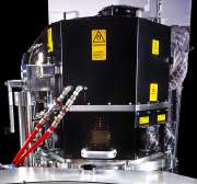 In the case of 300mm blanket etching for via reveal applications, however, the Rapier XE delivers the industry’s most productive process through the use of a patented dual source technology. This enhanced Rapier system is also available with ReVia, SPTS’ unique in-situ endpoint solution, that can monitor the via reveal process for extremely low (0.01%) via density and extremely low reveal heights (~1µm).
If you would like to know more about the specific capability of SPTS’ DSi-v or Rapier XE systems, please fill out our Online Enquiry Form
The link you have selected is located on another server. Neither SPTS Ltd. nor any of its subsidiaries endorses this web site, its sponsor, or any of the information, policies, activities, products, or services offered on the site or by any advertiser on the site. By clicking on the OK button below, you agree and acknowledge the foregoing and will be directed to the selected site.