
300mm PVD for Silicon Power Devices
Following announcements by various power device manufacturers[1] that they are moving to full-scale production on 300mm wafers, SPTS recently announced the availability of its field-proven PVD system that is configured to meet the needs of power applications. Currently, 7 out of the Top 10 Power IDMs and all major foundries rely on SPTS’s technology for power device PVD processes on 200 mm wafers.
In discrete power device manufacturing, current flows through the silicon, and consequently wafers receive contact metallization on both sides. SPTS’ Sigma® fxP PVD system covers both frontside thick metal processing, and backside metal deposition on thin wafers.
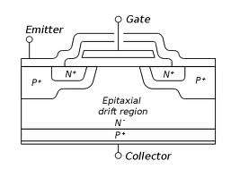
Cross-section of IGBT
To manage high device currents, thick aluminum alloy or copper layers are deposited on the front-side of the wafer (typically > 4 µm rather than <1 µm for mainstream silicon interconnects). However, depositing thick films puts unusually large heat loads on process chamber hardware, which can result in film contamination from outgassing chamber furniture. This contamination can lead to the formation of whiskers/extrusions in the growing film, producing device-killer defects. In traditional front end fab deposition equipment, a common technique to mitigate this issue is to reduce film deposition rates with a corresponding reduction on system productivity. However, the Sigma® fxP overcomes that challenge without compromising throughput. Customers routinely deposit thick metal layers at rates >1.4 µm/min without any yield-destroying whiskers or extrusions.
Following front-side processing, wafers are typically thinned down to < 100 µm to reduce ‘on-state’ resistance and solder metal layers are deposited on the backside. If no supporting carrier substrate is used, ultra-thin, large area wafers will deform under the influence of uncontrolled film stresses, which can cause wafer transport mishandling or device yield issues. The Sigma® fxP carries thin wafer handling hardware and uses film deposition stress control techniques to deliver high throughput processes with low wafer bow. To read more details about back-side metallization click here.
For more information on the Sigma® fxP, click here
References