
Via Reveal Processing
Through silicon vias (TSVs) are being implemented in place of traditional scaling for increasing device performance and reducing form factor. In addition to offering etch and deposition processes for the creation and lining of the via holes, SPTS processes can also be used for post-TSV steps, to prepare the die for connection to other parts of the device.
Via Reveal Process
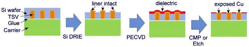
After completion of the front-side wafer processing (typically via middle) the wafer is temporarily bonded, face down, onto a carrier which can be glass or another silicon wafer. The active silicon is then ground typically to within 5-10 µm of the TSV nodes. After grinding the silicon is dry etched in a process that ‘reveals’ the vias to a step height of around 5 µm. After silicon etching the vias are passivated using a dielectric stack and then CMP’d (chemically mechanically polished) to expose the copper ready for RDL (redistribution layer) metallization.
Key Benefits of SPTS's Via Reveal Processes:
- REVIA® - unique end-pointing technique to monitor via reveal
- Silicon etch is highly selective to oxide liner - to prevent exposing the copper metal
- Dual plasma source with multi-mode operation - allows for uniformity tuning that can compensate for incoming wafer thickness variations
- Stable oxide and nitride passivation films can be deposited at low temperature (<180°C) with low stress and excellent mechanical/electrical properties
- Etch and deposition modules can be integrated to single fxP cluster platform to reduce cost of ownership for product development
For more details about SPTS etch and deposition products for via reveal processing, click links below: