
FOWLP - PVD Processes
Download this datasheet describing how fan-out wafer-level packaging (FOWLP) technology provides higher integration levels and a greater number of external contacts.
DownloadIntroduction
Fan-Out WLP (FOWLP) technology is an enhancement of standard wafer-level packages (WLPs) developed to provide a solution for semiconductor devices requiring a higher integration level and a greater number of external contacts. It provides a smaller package footprint with higher input/output (I/O) along with improved thermal and electrical performance.
In conventional WLP schemes I/O terminals are located over the chip surface area. Using this method, there is a limitation to the number of I/O connections.
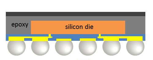
Fan-Out WLP (FOWLP) takes individual die and embeds them in a low cost material such as epoxy mold compound (EMC) with space allocated between each die for additional I/O connection points – avoiding the use of relatively expensive Si real estate to accommodate a high I/O count. Redistribution Layers (RDL) are formed using PVD seed deposition and subsequent electroplating/patterning to re-route I/O connections on the die to the mold compound regions in the periphery.
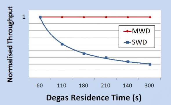
EMC is a cost-effective material for this application, but readily absorbs moisture when exposed to atmosphere. Outgassing during the PVD process sequence can have detrimental effects on device contact resistance (known as RC or RVIA) so an effective degas is essential. However, the material also has low thermal budget (<120°C) to prevent decomposition and excessive wafer warp. Consequently an effective degas requires low temperature and long process time - significantly reducing system throughput on traditional single wafer-based degas systems.
Improve Rc and Throughput
To eliminate the degas bottleneck challenge SPTS offer a “Multi-Wafer Degas” solution that enables a large number wafers to be degassed simultaneously before being individually transferred to subsequent pre-clean and sputter deposition without breaking vacuum. Wafers are dynamically pumped under clean, high vacuum conditions, with radiation heat transfer warming wafers directly to temperatures within the operating regimes for packaging applications.
A Sigma® fxP PVD system configured with MWD will deliver throughputs > 1.5x competitor systems based on single wafer degas processing technology. As materials emerge with even lower thermal budgets or schemes based on increased passivation thickness, longer degas times can be employed with no impact on throughput. Conversely, competitor systems based on single wafer degas will get progressively slower (see below).
Improved MWBC
With I/O counts increasing the amount of exposed metal contacts on the wafer present further challenges for MWBC. Standard over-etch practice to ensure all native oxide on contacts is removed will lead to a degree of metal contamination of the chamber walls. With ICP-based systems this leads to a breakdown of the RF coupling. In addition, the presence of organic passivation such as PI or PBO can lead to premature particle failure for chambers with insulating chamber walls due to the poor adhesion of organics to ceramic.
The SE-LTX pre-clean module is designed to provide ICP process capability yet overcome the process and particle stability challenges posed by increased I/O contacts and organics. Specialized hardware prevents continuous build-up of metal on the ceramic chamber walls and provides good chamber wall adhesion for organic passivation etch by-products, resulting in a typical particle performance with > 5000 wafers MWBC.
Cost-effective Cu Seed
With degas and pre-clean stages complete the final stage of the RDL seed process is the deposition of pre-plate seed layer themselves. Typically Ti or TiW adhesion/barrier layer followed by Cu seed, this stage of the process requires relatively uniform, repeatable metal films over low topography. Conventional PVD modules are used with Inspira PVD technology configured for lowest CoO - critical for back end processing.
Processing reconstituted wafers means wafer sizes are not necessarily limited to Si diameters and this presents opportunities for cost reduction. The Sigma fxP PVD solution has been designed to run larger format substrates, giving an increase in surface area for additional die to be processed in the same pass, reducing overall cost per die. Mold thickness can also be reduced, saving material cost. Wafer bows can increase as a result of either modification. As a result the Sigma® fxP has been designed to accommodate wafers with up to 10mm bow.
Information on this page contains forward looking information. For more information, click here.
The link you have selected is located on another server. Neither SPTS Ltd. nor any of its subsidiaries endorses this web site, its sponsor, or any of the information, policies, activities, products, or services offered on the site or by any advertiser on the site. By clicking on the OK button below, you agree and acknowledge the foregoing and will be directed to the selected site.