
Via Reveal Processing
High productivity plasma etch processes with unique end-point detection used for post-TSV steps, to prepare the die for connection to other parts of the device.
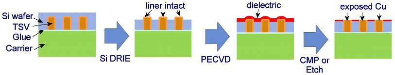
Via reveal occurs after the TSVs are formed, to prepare the vias for redistribution metallization. Wafers are temporarily bonded face-down to a carrier, and then thinned from the back side to reveal the vias. The via tips are then passivated, typically with a combination of silicon nitride and oxide before final CMP and redistribution metallization.
The temporary bonding adhesive between the substrate and carrier introduces two challenges to the PECVD passivation step:
The Delta fxP cluster system features a number of hardware and process innovations to deposit low leakage /high breakdown nitrides and TEOS oxides at low wafer temperature.
Excellent electrical isolation combined with high step coverage and controllable stress is obtained at wafer temperatures < 190°C. Critically, SPTS’ low temperature PECVD TEOS films are stable, with film properties staying constant over time (Fig 1).
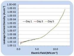
Fig 1
To ensure optimum film properties it is often necessary to degas the bonded wafer prior to PECVD passivation. An “ex-situ” anneal using a separate vacuum furnace is not effective because the bond adhesive will begin to reabsorb moisture as soon as it is exposed to air.
In-situ degas, where each wafer is passed from the degas chamber to the PECVD module without breaking vacuum provides the best results (Fig 2).
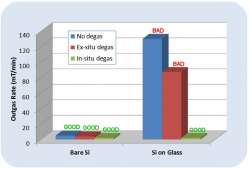
Fig 2
Since the temperature limit of bonded wafers is low, degas times of 15 minutes are not uncommon for some adhesives meaning significant cuts in productivity if a single wafer degas is adopted.
To address this “degas bottle-neck” in the process, SPTS’ Delta fxP can carry an integrated batch Multi-Wafer Degas [MWD] module. By degassing multiple wafers at the same time, degas times up to 1 hour can be accommodated without compromising system throughput.
SPTS is the only production supplier that configures dedicated degas modules on PECVD processing systems. For more information on SPTS's PECVD system, go to Products/PECVD
Information on this page contains forward looking information. For more information, click here
The link you have selected is located on another server. Neither SPTS Ltd. nor any of its subsidiaries endorses this web site, its sponsor, or any of the information, policies, activities, products, or services offered on the site or by any advertiser on the site. By clicking on the OK button below, you agree and acknowledge the foregoing and will be directed to the selected site.