
LPCVD SiN for MEMS
SPT's LPCVD SiN process that combines the excellent stress control and process repeatability of a PECVD process together with the benefits of low wet etch rate and low ownership cost of an LPCVD system
다운로드Low stress SiN is used in the manufacturing of MEMS devices as a structural material or an etch stop layer for the patterning of critical mechanical features. High and non-uniform stresses in the SiN film can cause undesirable deformation of the MEMS structures after release.
PECVD SiN is used for all applications which require a low (<400°C) deposition temperature, but where low deposition temperature is not a requirement, LPCVD SiN provides a less expensive alternative that delivers a film with a lower etch rate than the traditional PECVD.
In conventional LPCVD furnaces, gas depletion during the reaction causes variable film stress, which limits the viable batch size and reduces productivity. However, SPTS has developed a cost effective, low stress LPCVD SiN process that combines the excellent stress control and process repeatability of a PECVD process together with the low etch rate and low ownership cost of an LPCVD system. Available on the AVP/RVP vertical furnace, this process is able to repeatedly deliver a 100-wafer batch process with a stress variation of +/- 20 MPa together with wet etch rates <35 Å/min and excellent particle control. The use of low-cost batch processing enables around a 3x reduction in cost/wafer compared to competing LPCVD furnaces depending on the application requirements.
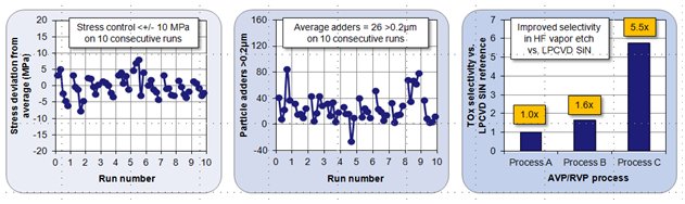
In addition, for oxide etch-stop applications, the technology has been proven to deliver >5x improvements in SiO2:SiN selectivity when using SPTS’ Primaxx HF vapor release etching, when compared to traditional LPCVD SiN.
With excellent process control, the AVP/RVP low stress SiN offers a viable cost-effective alternative to PECVD in applications where higher process temperatures can be tolerated. The low process costs and flexibility of the AVP/RVP platform enables multiple applications to be run without significantly adding to the overall production cost.
Key Benefits of SPTS' Low-Stress SiN Process:
For more details about SPTS LPCVD/diffusion process for MEMS applications, click 
The link you have selected is located on another server. Neither SPTS Ltd. nor any of its subsidiaries endorses this web site, its sponsor, or any of the information, policies, activities, products, or services offered on the site or by any advertiser on the site. By clicking on the OK button below, you agree and acknowledge the foregoing and will be directed to the selected site.