
WL Packaging of MEMS
Wafer level packaging (WLP) prior to wafer dicing of MEMS devices can provide protection from particles and dicing slurry, while significantly reducing form factor and reducing the overall die cost.
다운로드Micro electro mechanical systems (MEMS) devices, also known as micromachines, are typically fragile, often containing moving parts that can be damaged during dicing. Wafer level packaging (WLP) prior to wafer dicing can provide protection from particles and dicing slurry, while significantly reducing form factor and reducing the overall die cost.
Increasingly, many MEMS devices, such as microsensors, require a vacuum or controlled atmosphere for operation. This could be used to control parameters such as the Q-factor (amount of damping), or to provide a reference vacuum for pressure sensors, or to reduce absorption in infrared sensors and improve sensitivity and resolution. Two such examples of wafer level packaging are silicon capping and thin film encapsulation, each providing benefits for specific packaging applications.
One common method of packaging micromachined devices is to bond a silicon cap wafer to the device wafer. This can be used for multiple sensors on the same die, utilizes metal-eutectic bonding and requires less bonding area than traditional glass frit capping. Through silicon vias (TSVs) can be used instead of I/O pads – further reducing form factor size.
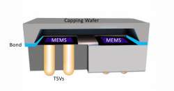
Fig.1 Schematic illustration of capping wafer bonded to MEMS wafer
A lower cost and simpler packaging alternative is thin film encapsulation. By eliminating the need for sealing/bonding and a capping wafer, thin film encapsulation is, for some MEMS designs, the simplest and lowest cost packaging alternative.
The technique uses a double sacrificial layer (normally silicon or silicon oxide) which supports the MEMS structure and defines a space above the structure while a cap layer is deposited over the device layer (Fig.s 2 & 3).
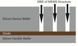
Fig. 2 Silicon DRIE to define MEMS structure
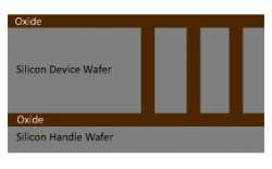
Fig. 3 Oxide deposition to support MEMS structure
Holes in the capping layer allow an etchant (e.g vapor HF or XeF2 depending on the sacrificial material) to remove the sacrificial layer and “release” the moving MEMS structure (see Fig 4 & 5).
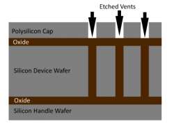
Fig. 4 Silicon DRIE of vents through polysilicon cap
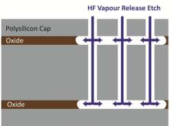
Fig. 5 HF vapor release etch
These holes must then be closed by depositing a final sealing layer. Typical sealing materials include epi- or LPCVD PolySi , PECVD SiOx or SiNy or metals such as aluminium (Fig. 6)
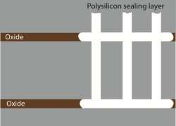
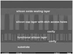
Fig. 7 Si MEMS device, released using vapor HF, capped with silicon and sealed with oxide (SUMICAP Project)
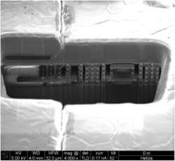
Fig. 8 CMOS-MEMS device released with vapour HF and sealed with thick Al layer
(Courtesy of BAOLAB Microsystems)
Ideally, the device package should be sealed without removing the wafer from vacuum, to avoid yield or performance loss from unwanted absorption of contaminating gases or moisture. Different MEMS devices require different cavity pressures, and the required pressure/gas composition can be tailored prior to sealing. Stress, temperature and vacuum requirements will determine optimum sealing material.
SPTS Technologies offers customers the complete range of processes required for thin film encapsulation of MEMS devices:
The link you have selected is located on another server. Neither SPTS Ltd. nor any of its subsidiaries endorses this web site, its sponsor, or any of the information, policies, activities, products, or services offered on the site or by any advertiser on the site. By clicking on the OK button below, you agree and acknowledge the foregoing and will be directed to the selected site.