
Etch and Deposition Solutions for Advanced Packaging
As the semiconductor industry looks beyond “Moore’s Law”, with dimensional scaling reaching its physical limits, new solutions are being developed to reduce chip size/height and lower production costs, while improving reliability, energy efficiency, device speed and multi-function integration.
SPTS Technologies offers a range of plasma etch and deposition process technologies being used by leading semiconductor packaging companies for advanced packaging schemes - from High Density Fan-Out Wafer Level Packaging (FOWLP) to the most advanced "3D" packages where two or more die, potentially for different functions, are stacked and connected in the vertical direction with through-silicon vias (TSV) filled with metal.
Leveraging our decades of expertise in deep silicon etching of MEMS and TSVs, SPTS also offers the most advanced plasma dicing solutions for dicing before grind (DBG) or dicing after grind (DAG) of wafers up to 300mm in diameter.
Silicon Etching
The Omega® range of plasma etch systems includes the Rapier™ process module for high rate silicon etching in advanced packaging applications. Vertical or tapered, high aspect ratio via holes or slots can be created through silicon wafers or interposers which, once filled with conducting metals such as copper, form interconnects between different layers in the 2.5D/3D-IC package.
Blanket via reveal etching is required to expose the Cu-filled vias from the backside of the wafer, prior to connection. The Rapier™ XE process module combines recipe tuneable uniformity with an etch rate that is typically 2-4 times faster than competing systems for a blanket silicon etch. The same process can be used for extreme wafer thinning down to 5µm or even 0.5µm through the incorporation of an etch stop layer.
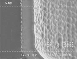
Blanket silicon on the backside of a wafer reveals the base tips of the TSVs
SPTS also offers unique, patent-protected end-point solutions for TSV etching, via reveal and extreme thinning processes which enable optimal throughput and yields in high volume production.
PECVD for Low Temperature Dielectric Deposition
For advanced packaging applications, SPTS's Delta™ PECVD system offers low temperature deposition processes compatible with 300mm bonded substrates and mold. Applications include via-last TSV liner, via-reveal passivation and fusion bond.
Delta™ PECVD produces high quality, production qualified SiO and SiN films at deposition temperatures as low as 110°C. SiN – SiO stacks can be deposited in the same PECVD chamber with unrivalled electrical performance and stability over time. Film and stack stress can be tuned across a wide range and optimised chamber hardware enables the lowest within-wafer stress range over competing PECVD system. Where required, single-wafer and multi-wafer degas options are available to heat outgassing substrates and improve deposited film quality.
Optimized SiO, TEOS SiO and other advanced dielectric films are available for fusion bonding applications.
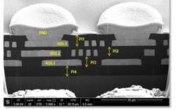
PECVD oxide barrier near the base of a TSV
Physical Vapor Deposition (PVD) for Metal Deposition
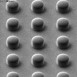
The Sigma® PVD systems are used to deposit metals such as Au, Al, Ti, TiW and Cu, on Si or mold wafers. The adoption of organic passivation and new substrate materials for advanced packaging technologies present technical challenges for UBM/RDL. Using novel degas and pre-clean technology, the Sigma® fxP produces consistently low Rc values whilst delivering a 2x throughput advantage over other PVD systems. In 2.5D and 3D-IC applications, SPTS' Advanced Hi-Fill Ionized PVD source delivers world-class Cu barrier/seed coverage in high aspect ratio TSVs.
PVD-deposited re-distribution layers (RDL) in FOWLP structure
Plasma Dicing
The Mosaic™ plasma dicing systems offer an alternative to mechanical saw or laser technologies, for singulation of die from a silicon wafer (up to 300mm, on frames). This solution offers a low damage, dry chemical process which increases die strength and avoids particulate contamination. These benefits are especially important when the wafers are thin or contain fragile low k films and for die to wafer bonding. Being a parallel process, it can offer significant throughput, yield and cost advantages when dicing small die and/or thin wafers. Dicing lanes are defined by a mask and can be much narrower than the equivalent lanes for saws or lasers, allowing more die per wafer. Additionally the dicing lanes need not be straight lines, offering more freedom for die shape/size and optimized wafer layouts.
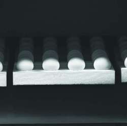
Bumped die on tape, singulated by plasma dicing
If you would like to find out more about our processing capabilities for Advanced Packaging applications, please Contact Us