
Plasma Processes for Photonic Devices
Download this datasheet giving an overview of SPTS's etch and deposition processes used to manufacture a range of photonic products such as LEDS, optical waveguides, VCSELs and lasers.
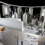
DownloadSPTS offers PVD processes depositing metals on compound semiconductor substrates for VCSELs, LEDs and other optoelectronic devices, along with 300 mm Si for Integrated Photonics Advanced Packaging. Applications include diffusion barriers, Au interconnect, stress compensation layers and Si UBM/RDL.
The link you have selected is located on another server. Neither SPTS Ltd. nor any of its subsidiaries endorses this web site, its sponsor, or any of the information, policies, activities, products, or services offered on the site or by any advertiser on the site. By clicking on the OK button below, you agree and acknowledge the foregoing and will be directed to the selected site.