
Plasma Dicing
Stronger die - more die. High yield plasma dicing solutions based on industry leading Deep Reactive Ion Etch (DRIE) technology for dice-before-grind and dice-after-grind.
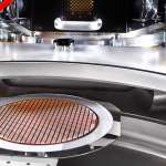
DownloadPlasma dicing, using Deep Reactive Ion Etching (DRIE) processing, is gaining rapid acceptance within the semiconductor industry as a viable alternative to conventional singulation methods using saw blades or LASERs.
Plasma dicing offers considerable benefits to users
Plasma dicing can be carried out before grinding, where deep dicing lanes are etched into the wafer and the die are singulated by a final backside grind operation, or after grind where DRIE is used to etch through thinned wafers mounted on taped frames, or carriers.
Plasma dicing is compatible with solder bumps and backside metal, and the Mosaic™ plasma dicing solution has successfully demonstrated “dicing after grind” on standard/thinned/TAIKO wafers and wafer pieces, on a range of dicing frames and tapes.
The link you have selected is located on another server. Neither SPTS Ltd. nor any of its subsidiaries endorses this web site, its sponsor, or any of the information, policies, activities, products, or services offered on the site or by any advertiser on the site. By clicking on the OK button below, you agree and acknowledge the foregoing and will be directed to the selected site.