
Via Reveal Processing
High productivity plasma etch processes with unique end-point detection used for post-TSV steps, to prepare the die for connection to other parts of the device.
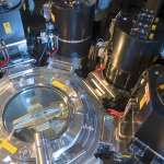
Through-silicon via (TSV) technology is currently being implemented across a broad range of device types. TSV has the potential to reduce form-factors, increases performance and enable heterogeneous integration.
TSV etching, at depths typically in the 50-200µm range, requires the use of the Bosch process for best control over the wall profile and mask selectivity. Also critical is the via reveal process that exposes the TSV nodes for the subsequent redistribution layer (RDL) metallisation. To perform via reveal, the user grinds the wafer from the backside to a point some 10 to 15µm above the tips of the buried TSV’s. The same Si surface is then dry etched to expose the via tips and leave them proud of the Si surface by approximately 5µm – the “via reveal”.
The link you have selected is located on another server. Neither SPTS Ltd. nor any of its subsidiaries endorses this web site, its sponsor, or any of the information, policies, activities, products, or services offered on the site or by any advertiser on the site. By clicking on the OK button below, you agree and acknowledge the foregoing and will be directed to the selected site.