
Introduction to Si DRIE
Brief introduction to silicon DRIE (The Bosch Process) and its application within MEMS, Advanced Packaging and Power Device manufacturing.
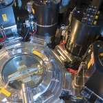
DownloadThe key building block in MEMS fabrication is deep silicon (Si) etching; with processes including high rate etching, high aspect ratio, through-wafer etches and etching to buried oxide layers, including SOI wafers.
A patented dual plasma source arrangement produces uniform plasma density in the chamber which improves profile/depth uniformity and controls profile tilting.
A patented thick dielectric electrostatic chuck (ESC) allows wafer-less plasma cleans for best process stability and clamping through carriers, such as glass.
The industry’s highest productivity metrics can be achieved on SPTS’ DRIE equipment, with high uptimes and mean time between clean (MTBC).
The link you have selected is located on another server. Neither SPTS Ltd. nor any of its subsidiaries endorses this web site, its sponsor, or any of the information, policies, activities, products, or services offered on the site or by any advertiser on the site. By clicking on the OK button below, you agree and acknowledge the foregoing and will be directed to the selected site.