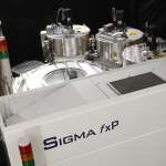
PVD for Power Devices

SPTS offers metal deposition solutions for two key areas of power device manufacture: thick frontside metal & thin wafer backside metallization – both on 200 mm and 300 mm platforms.

Benefits of SPTS PVD for Frontside Power Applications

  • High Throughput thick Al with low defect levels – reduced CoO with highest yield
  • 2x throughput increase. 30% CoO reduction.
  • 50% fewer systems to hit capacity target
  • Long target/shield life with fast chamber recovery, maximizing uptime

Benefits of SPTS PVD for Power Backside Metal

  • Same basic hardware as frontside processing configuration
  • Specialised hardware prevents active face damage
  • Multiple stress control parameters enable efficient management of wafer bow

Related Product Information