
Introduction to Si DRIE
Brief introduction to silicon DRIE (The Bosch Process) and its application within MEMS, Advanced Packaging and Power Device manufacturing.
下載As the semiconductor industry looks beyond “Moore’s Law”, with dimensional scaling reaching its physical limits, new solutions are being developed to reduce chip size/height and lower production costs, while improving reliability, energy efficiency, device speed and multi-function integration. These attributes are becoming more essential, particularly in the field of high performance computing, not only in the traditional server and data farm applications, but also in more space-sensitive applications such as autonomous cars, Industry 4.0, and other emerging “Big Data” applications.
There are many different approaches and solutions trying to achieve this which are commonly grouped under the category of “Advanced Packaging”. These solutions are essentially all designed to integrate different types of chips (e.g. memory, logic, sensors, etc) as close to each other as possible, in a single package, sometimes referred to as heterogeneous integration, and in a way that is reliable and cost-efficient in high volume production. Such solutions include:
 (i) High Density FOWLP
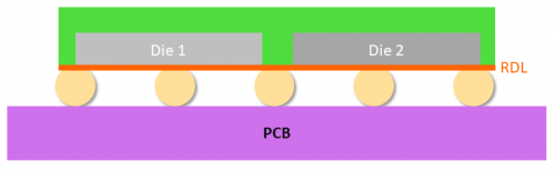
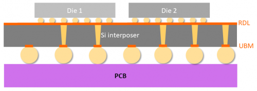 (ii) 2.5D Package with Silicon Interposer
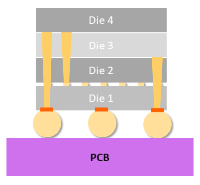 (iii) 3D-TSV Package
SPTS Technologies offers a range of plasma etch and deposition processes that are being used by leading packaging companies in high volume manufacture. We have been working with customers to develop leading-edge 2.5D/3D TSV solutions for over a decade, and we have a broad range of production-proven processes and know-how to help customers implement these technologies in high volume manufacturing.
Via Etch
The Omega® range of plasma etch systems includes the Rapier™ process module for high rate silicon etching in advanced packaging applications. Vertical or tapered, high aspect ratio via holes or slots can be created through silicon wafers or interposers which, once filled with conducting metals such as copper, form interconnects between different layers in the 2.5D/3D-IC package.
SPTS has been leading the way in deep reactive ion etching (DRIE) since this technology was invented to manufacture silicon-based MEMS devices in the mid 1990’s. In addition to industry-leading etch rates and profile control, we also offer Claritas™, a unique end-point technology which allows reliable end-pointing of silicon via etch processes even at low via densities (<0.5% open area).
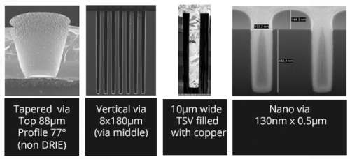
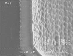
Selected examples of various TSV structures
Via Liner Deposition
Before the via can be filled with copper, it is necessary to coat the inside of the hole with a dielectric “liner” to confine the electrical current within the via connection. SPTS’s Delta™ PECVD system offers the capability to deposit oxide using both silane and tetraethyl orthosilicate (TEOS). However, it has been found that for higher aspect ratio TSVs TEOS gives a much better sidewall coverage, and it exhibits superior electrical characteristics with low leakage values and high electrical breakdown fields.
PECVD oxide barrier near the base of a TSV
Via Barrier/Seed Deposition
Before the lined via can be filled with Cu, there is also a need for a barrier layer, typically TaN, Ti, TiN, to prevent any chance of Cu atoms migrating through the dielectric into the silicon substrate, and then a Cu seed layer is deposited to create good adhesion to the barrier layer and facilitate the subsequent electrochemical deposition step used to finally fill the via with Cu. Both the barrier and seed layers can be deposited using Sigma® PVD Advanced Hi-Fill® module utilizing ionized PVD technology to achieve deposition into "via-last" TSVs (up to ~10:1) by promoting the re-sputtering of metals into “hidden” areas on the sidewall.
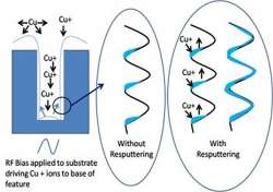
Comparison of standard PVD versus ionised PVD which resputters material to improve coating areas hidden from the "line-of-sight" of the normal PVD bombardment.
Via Reveal
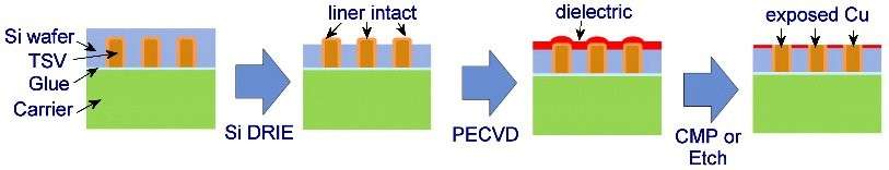
After the via is filled, the wafer is bonded face-down to a carrier wafer and thinned using a combination of grinding and CMP. Blanket silicon etching is required to expose the Cu-filled vias from the backside of the wafer, prior to connection. The Rapier™ XE process module combines recipe tuneable uniformity with an etch rate that is typically 2-4 times faster than competing systems, and our ReVia® end-point enables accurate, automated process control for high yields.
In some cases, it may be possible to use grinding and plasma etch alone, eliminating the expensive CMP processing. Contact us for more details.
The reveal via tips are then coated with low temperature PECVD dielectric where processing temperature is limited (<180°C) due to the temporary bond with the carrier wafer and stress control is paramount to prevent excessive wafer bow after de-bonding. Learn more about the competitive advantages of using the Delta™ fxP for this passivation step in this Tech Insight.
More details about the via reveal process is shared in our Via Reveal Tech Insight.
Wafer Thinning
In addition to via reveal processing described above, there are a number of other wafer thinning applications, where the blanket silicon etch capabilities of the Rapier™ XE can be utilized. These include:
[1] A. Jourdain et al., "Extreme Wafer Thinning and nano-TSV processing for 3D Heterogeneous Integration," 2020 IEEE 70th Electronic Components and Technology Conference (ECTC), Orlando, FL, USA, 2020, pp. 42-48, doi: 10.1109/ECTC32862.2020.00020.
The link you have selected is located on another server. Neither SPTS Ltd. nor any of its subsidiaries endorses this web site, its sponsor, or any of the information, policies, activities, products, or services offered on the site or by any advertiser on the site. By clicking on the OK button below, you agree and acknowledge the foregoing and will be directed to the selected site.